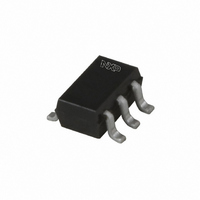
74LVC1G18GW,125 NXP Semiconductors, 74LVC1G18GW,125 Datasheet - Page 3

74LVC1G18GW,125
Manufacturer Part Number
74LVC1G18GW,125
Description
IC 1OF2 NON-INV DEMUX 3ST SC-88
Manufacturer
NXP Semiconductors
Series
74LVCr
Type
Demultiplexerr
Datasheet
1.74LVC1G18GV125.pdf
(13 pages)
Specifications of 74LVC1G18GW,125
Package / Case
SC-70-6, SC-88, SOT-363
Circuit
1 x 1:2
Independent Circuits
1
Current - Output High, Low
32mA, 32mA
Voltage Supply Source
Single Supply
Voltage - Supply
1.65 V ~ 5.5 V
Operating Temperature
-40°C ~ 125°C
Mounting Type
Surface Mount
Logic Family
LVC
Number Of Lines (input / Output)
1.0 / 2.0
Propagation Delay Time
50 ns
Supply Voltage (max)
5.5 V
Supply Voltage (min)
1.65 V
Maximum Operating Temperature
+ 125 C
Minimum Operating Temperature
- 40 C
Mounting Style
SMD/SMT
Number Of Input Lines
1.0
Number Of Output Lines
2.0
Lead Free Status / RoHS Status
Lead free / RoHS Compliant
Lead Free Status / RoHS Status
Lead free / RoHS Compliant, Lead free / RoHS Compliant
Other names
74LVC1G18GW-G
74LVC1G18GW-G
935273781125
74LVC1G18GW-G
935273781125
NXP Semiconductors
7. Functional description
Table 4.
[1]
8. Limiting values
Table 5.
In accordance with the Absolute Maximum Rating System (IEC 60134). Voltages are referenced to GND (ground = 0 V).
[1]
[2]
[3]
9. Recommended operating conditions
Table 6.
74LVC1G18_2
Product data sheet
Input
S
L
L
H
H
Symbol
V
I
V
I
V
I
I
I
T
P
Symbol
V
V
V
T
IK
OK
O
CC
GND
stg
amb
t/ V
CC
I
O
tot
CC
I
O
H = HIGH voltage level; L = LOW voltage level; Z = high-impedance OFF-state
The input and output voltage ratings may be exceeded if the input and output current ratings are observed.
When V
For SC-74 and SC-88 packages: above 87.5 C the value of P
CC
Function table
Limiting values
Recommended operating conditions
Parameter
supply voltage
input clamping current
input voltage
output clamping current
output voltage
output current
supply current
ground current
storage temperature
total power dissipation
Parameter
supply voltage
input voltage
output voltage
ambient temperature
input transition rise and fall rate
= 0 V (Power-down mode), the output voltage can be 5.5 V in normal operation.
[1]
A
L
H
L
H
Conditions
V
V
Active mode
Power-down mode
V
T
1-of-2 non-inverting demultiplexer with 3-state deselected output
Conditions
Active mode
V
V
V
amb
I
O
O
< 0 V
CC
CC
CC
Rev. 02 — 30 August 2007
> V
= 0 V to V
=
= 0 V; Power-down mode
= 1.65 V to 2.7 V
= 2.7 V to 5.5 V
CC
40 C to +125 C
or V
tot
CC
O
derates linearly with 4.0 mW/K.
Output
1Y
L
H
Z
Z
< 0 V
[1][2]
[1][2]
[1]
[3]
Min
1.65
0
0
0
-
-
40
Min
-
-
-
-
0.5
50
0.5
0.5
0.5
100
65
2Y
Z
Z
L
H
Typ
-
-
-
-
-
-
-
74LVC1G18
Max
+6.5
-
+6.5
V
+6.5
100
-
+150
300
50
50
© NXP B.V. 2007. All rights reserved.
CC
Max
5.5
5.5
V
5.5
+125
20
10
+ 0.5
CC
Unit
V
V
V
V
ns/V
ns/V
Unit
V
mA
V
mA
V
V
mA
mA
mA
mW
C
C
O
O
3 of 13


