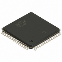
CY7C4811-10AC Cypress Semiconductor Corp, CY7C4811-10AC Datasheet - Page 19

CY7C4811-10AC
Manufacturer Part Number
CY7C4811-10AC
Description
IC SYNC FIFO 512X9X2 64LQFP
Manufacturer
Cypress Semiconductor Corp
Series
CY7Cr
Datasheet
1.CY7C4811-10AC.pdf
(23 pages)
Specifications of CY7C4811-10AC
Function
Synchronous, Dual Port
Memory Size
9.2K (512 x 9 x 2)
Data Rate
100MHz
Access Time
8ns
Voltage - Supply
3.3V
Operating Temperature
-40°C ~ 85°C
Mounting Type
Surface Mount
Package / Case
64-LQFP
Lead Free Status / RoHS Status
Contains lead / RoHS non-compliant
Other names
428-1256
Available stocks
Company
Part Number
Manufacturer
Quantity
Price
Company:
Part Number:
CY7C4811-10AC
Manufacturer:
CY
Quantity:
8
Company:
Part Number:
CY7C4811-10AC
Manufacturer:
CYPRESS
Quantity:
11
Company:
Part Number:
CY7C4811-10AC
Manufacturer:
CYPRESS
Quantity:
717
Bidirectional Configuration
The two FIFOs of the CY7C4801/4811/4821/4831/4841/4851
can be used to buffer data flow in two directions. In the exam-
ple that follows, processor A can write data to processor B via
Depth Expansion
CY7C4801/4811/4821/4831/4841/4851can be adapted to ap-
plications that require greater than 256/512/1024/2048/4096/
8192 words. The existence of dual enable pins on the read and
write ports allow depth expansion. The Write Enable 2/Load
(WENA2, WENB2) pins are used as a second write enables in
a depth expansion configuration, thus the Programmable flags
are set to the default values. Depth expansion is possible by
using one enable input for system control while the other en-
able input is controlled by expansion logic to direct the flow of
Document #: 38-06005 Rev. **
PROCESSOR A
CONTROL
ADDRESS
RAM
CLOCK
DATA
9
9
Figure 4. Block Diagram of Bidirectional Configuration.
V
CC
9
9
WENA2
WCLKA
WENA1
DA
RCLKB
RENB1
OEB
QB
RENB2
RAM ARRAY B
RAM ARRAY A
0
0
CY7C4851
DA
CY7C4801
CY7C4811
CY7C4821
CY7C4831
CY7C4841
QB
8
8
QA
DB
WENB1
WCLKB
WENB2
RENA2
RCLKA
RENA1
0
0
OEA
FIFO A, and, in turn, processor B can write processor A via
FIFO B.
data. a typical application would have the expansion logic al-
ternate data access from one device to the next in a sequential
manner. The CY7C4801/4811/4821/4831/4841/ 4851 oper-
ates in the Depth Expansion configuration when the following
conditions are met:
QA
DB
1. WENA2/LDA and WENB2/LDB pins are held HIGH during
2. External logic is used to control the flow of data.
V
Reset so that these pins operate as second Write Enables.
8
8
CC
9
9
CY7C4831/4841/4851
CY7C4801/4811/4821
9
9
PROCESSOR A
CLOCK
ADDRESS
CONTROL
DATA
RAM
48X1–18
Page 19 of 23


