IDT72V241L10PF IDT, Integrated Device Technology Inc, IDT72V241L10PF Datasheet - Page 8
IDT72V241L10PF
Manufacturer Part Number
IDT72V241L10PF
Description
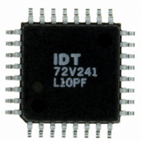
IC FIFO SYNC 4KX9 10NS 32QFP
Manufacturer
IDT, Integrated Device Technology Inc
Series
72Vr
Datasheet
1.IDT72V221L15PFG.pdf
(14 pages)
Specifications of IDT72V241L10PF
Function
Synchronous
Memory Size
36K (4K x 9)
Access Time
10ns
Voltage - Supply
3 V ~ 3.6 V
Operating Temperature
0°C ~ 70°C
Mounting Type
Surface Mount
Package / Case
32-TQFP, 32-VQFP
Configuration
Dual
Density
36Kb
Access Time (max)
6.5ns
Word Size
9b
Organization
4Kx9
Sync/async
Synchronous
Expandable
Yes
Bus Direction
Uni-Directional
Package Type
TQFP
Clock Freq (max)
100MHz
Operating Supply Voltage (typ)
3.3V
Operating Supply Voltage (min)
3V
Operating Supply Voltage (max)
3.6V
Supply Current
20mA
Operating Temp Range
0C to 70C
Operating Temperature Classification
Commercial
Mounting
Surface Mount
Pin Count
32
Lead Free Status / RoHS Status
Contains lead / RoHS non-compliant
Data Rate
-
Lead Free Status / RoHS Status
Not Compliant, Contains lead / RoHS non-compliant
Other names
72V241L10PF
800-1518
800-1518
Available stocks
Company
Part Number
Manufacturer
Quantity
Price
Company:

Part Number:
IDT72V241L10PF
Manufacturer:
IDT, Integrated Device Technology Inc
Quantity:
10 000
Company:
Part Number:
IDT72V241L10PF8
Manufacturer:
IDT, Integrated Device Technology Inc
Quantity:
10 000
Company:
Part Number:
IDT72V241L10PFG
Manufacturer:
IDT, Integrated Device Technology Inc
Quantity:
10 000
Part Number:
IDT72V241L10PFG
Manufacturer:
IDT
Quantity:
20 000
Company:
Part Number:
IDT72V241L10PFG8
Manufacturer:
IDT, Integrated Device Technology Inc
Quantity:
10 000


NOTES:
1. Holding WEN2/LD HIGH during reset will make the pin act as a second write enable pin. Holding WEN2/LD LOW during reset will make the pin act as a load enable for the programmable
2. After reset, the outputs will be LOW if OE = 0 and high-impedance if OE = 1.
3. The clocks (RCLK, WCLK) can be free-running during reset.
NOTE:
1. t
(If Applicable)
IDT72V201/72V211/72V221/72V231/72V241/72V251 3.3V CMOS SyncFIFO™
256 x 9, 512 x 9, 1,024 x 9, 2,048 x 9, 4,096 x 9 and 8,192 x 9
WEN2/LD
flag offset registers.
the rising edge of RCLK and the rising edge of WCLK is less than t
EF, PAE
FF, PAF
SKEW1
Q
REN1,
WEN1
REN2
0
D
WEN2/
WCLK
- Q
WEN1
REN1,
RCLK
REN2
0
RS
is the minimum time between a rising RCLK edge and a rising WCLK edge for FF to change during the current clock cycle. If the time between
- D
8
FF
(1)
8
t
SKEW1 (1)
t
t
t
CLKH
t
RSF
RSF
RSF
t
WFF
t
RS
DATA IN VALID
t
t
t
RSS
RSS
RSS
Figure 5. Write Cycle Timing
t
SKEW1
CLK
Figure 4. Reset Timing
, then FF may not change state until the next WCLK edge.
t
CLKL
t
8
t
ENS
ENS
t
DS
COMMERCIAL AND INDUSTRIAL
t
t
t
ENH
DH
ENH
t
t
t
TEMPERATURE RANGES
RSR
RSR
RSR
t
WFF
NO OPERATION
NO OPERATION
OE = 1
OE = 0
COMMERCIAL AND INDUSTRIAL
(2)
TEMPERATURE RANGES
OCTOBER 22, 2008
4092 drw07
4092 drw06
Related parts for IDT72V241L10PF
Image
Part Number
Description
Manufacturer
Datasheet
Request
R

Part Number:
Description:
TRANSLATION DEVICE DPI 80-PQFP
Manufacturer:
IDT, Integrated Device Technology Inc
Datasheet:
Part Number:
Description:
IDT PART
Manufacturer:
IDT, Integrated Device Technology Inc
Datasheet:
Part Number:
Description:
IC LIU T1/E1/J1 OCTAL 256PBGA
Manufacturer:
IDT, Integrated Device Technology Inc
Datasheet:

Part Number:
Description:
IC FREQ TIMING GENERATOR 28TSSOP
Manufacturer:
IDT, Integrated Device Technology Inc
Datasheet:
Part Number:
Description:
IC CLK DVR PLL 1:10 40VFQFPN
Manufacturer:
IDT, Integrated Device Technology Inc
Datasheet:
Part Number:
Description:
IC CLK FANOUT BUFFER 1:18 32LQFP
Manufacturer:
IDT, Integrated Device Technology Inc
Datasheet:
Part Number:
Description:
IC CLK FANOUT BUFFER 1:18 32LQFP
Manufacturer:
IDT, Integrated Device Technology Inc
Datasheet:
Part Number:
Description:
IC CK505 VREG/RES 56TSSOP
Manufacturer:
IDT, Integrated Device Technology Inc
Datasheet:

Part Number:
Description:
IC SDRAM CLK DVR 1:10 48-TSSOP
Manufacturer:
IDT, Integrated Device Technology Inc
Datasheet:

Part Number:
Description:
IC CLK DVR PLL 1:10 48TSSOP
Manufacturer:
IDT, Integrated Device Technology Inc
Datasheet:
Part Number:
Description:
IC FLEXPC CLK PROGR P4 56-TSSOP
Manufacturer:
IDT, Integrated Device Technology Inc
Datasheet:
Part Number:
Description:
IC FLEXPC CLK PROGR P4 56-TSSOP
Manufacturer:
IDT, Integrated Device Technology Inc
Datasheet:
Part Number:
Description:
IC FLEXPC CLK PROGR P4 56-SSOP
Manufacturer:
IDT, Integrated Device Technology Inc
Datasheet:

Part Number:
Description:
IC PLL CLK DRIVER 2.5V 28-TSSOP
Manufacturer:
IDT, Integrated Device Technology Inc
Datasheet:
Part Number:
Description:
IC CLOCK DRIVER 2.5V 24-TSSOP
Manufacturer:
IDT, Integrated Device Technology Inc
Datasheet: