AD734AQ Analog Devices Inc, AD734AQ Datasheet - Page 9
AD734AQ
Manufacturer Part Number
AD734AQ
Description
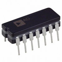
IC MULTIPLIER/DIVIDER 14-CDIP
Manufacturer
Analog Devices Inc
Datasheet
1.AD734AQ.pdf
(12 pages)
Specifications of AD734AQ
Rohs Status
RoHS non-compliant
Function
Analog Multiplier
Number Of Bits/stages
4-Quadrant
Package / Case
14-CDIP (0.300", 7.62mm)
No. Of Multipliers / Dividers
1
No. Of Amplifiers
4
Supply Voltage Range
± 8V To ± 16.5V
Slew Rate
450V/µs
Operating Temperature Range
-40°C To +85°C
Digital Ic Case Style
DIP
Lead Free Status / RoHS Status
Contains lead / RoHS non-compliant
Available stocks
Company
Part Number
Manufacturer
Quantity
Price


A PRECISION AGC LOOP
The variable denominator of the AD734 and its high gain-
bandwidth product make it an excellent choice for precise
automatic gain control (AGC) applications. Figure 13 shows a
suggested method. The input signal, E
peak amplitude of from 10 mV to 10 V at any frequency from
100 Hz to 10 MHz, is applied to the X input, and a fixed posi-
tive voltage E
form an integrator having a current summing node at its invert-
ing input. (The AD712 dual op amp is a suitable choice for this
application.) In the absence of an input, the current in D2 and
R2 causes the integrator output to ramp negative, clamped by
diode D3, which is included to reduce the time required for the
loop to establish a stable, calibrated, output level once the
circuit has received an input signal. With no input to the
denominator (U0 and U2), the gain of the AD734 is very high
(about 70 dB), and thus even a small input causes a substantial
output.
Diode D1 and C1 form a peak detector, which rectifies the out-
put and causes the integrator to ramp positive. When the
current in R1 balances the current in R2, the integrator output
holds the denominator output at a constant value. This occurs
when there is sufficient gain to raise the amplitude of E
required to establish an output amplitude of E
of +1 V to +10 V. The X input of the AD734, which has finite
offset voltage, could be troublesome at the output at high gains.
The output offset is reduced to that of the X input (one or two
millivolts) by the offset loop comprising R3, C3, and buffer A1.
The low pass corner frequency of 0.16 Hz is transformed to a
high-pass corner that is multiplied by the gain (for example,
160 Hz at a gain of 1000).
In applications not requiring operation down to low frequencies,
amplifier A1 can he eliminated, but the AD734’s input
resistance of 50 k between X1 and X2 will reduce the time
constant and increase the input offset. Using a non-polar 20 F
tantalum capacitor for C1 will result in the same unity-gain
high-pass corner; in this case, the offset gain increases to 20, still
very acceptable.
Figure 14 shows the error in the output for sinusoidal inputs at
100 Hz, 100 kHz, and 1 MHz, with E
put error for any frequency between 300 Hz and 300 kHz is
similar to that for 100 kHz. At low signal frequencies and low
input amplitudes, the dynamics of the control loop determine
the gain error and distortion; at high frequencies, the 200 MHz
gain-bandwidth product of the AD734 limit the available gain.
REV. C
+1V TO
1N914
+10V
E
E
IN
C
D3
1 F
1 F
C1
C2
D2
1N914
1M
C
R2
Figure 13. Precision AGC Loop
to the Y input. Op amp A2 and capacitor C2
A2
A1
1M
R1
NC
1
2
3
4
5
6
7
X1
X2
U0
U1
U2
Y1
Y2
AD734
1M
R3
DD
VP
ER
VN
Z2
Z1
W
14
13
12
11
10
9
8
C
IN
set to +10 V. The out-
, which may have a
+15V
–15V
OP AMP = AD712 DUAL
0.1 F
0.1 F
L
C
over the range
1N914
1 F
D1
C1
L
IN
to that
E
OUT
–9–
The output amplitude tracks E
more than +10 V.
WIDEBAND RMS-DC CONVERTER
USING U INTERFACE
The AD734 is well suited to such applications as implicit RMS-
DC conversion, where the AD734 implements the function
using its direct divide mode. Figure 15 shows the circuit.
In this application, the AD734 and an AD708 dual op amp
serve as a 2-chip RMS-DC converter with a 10 MHz bandwidth.
Figure 16 shows the circuit’s performance for square-, sine-,
and triangle-wave inputs. The circuit accepts signals as high as
10 V p-p with a crest factor of 1 or 1 V p-p with a crest factor of
10. The circuit’s response is flat to 10 MHz with an input of
10 V, flat to almost 5 MHz for an input of 1 V, and to almost
1 MHz for inputs of 100 mV. For accurate measurements of
input levels below 100 mV, the AD734’s output offset (Z inter-
face) voltage, which contributes a dc error, must be trimmed out.
In Figure 15’s circuit, the AD734 squares the input signal, and
its output (V
R1 and C1 and has a corner frequency of 1 Hz. Because of the
implicit feedback loop, this value is both the output value, V
and the denominator in Equation (13). U2a and U2b, an
AD708 dual dc precision op amp, serve as unity-gain buffers,
supplying both the output voltage and driving the U interface.
Figure 14. AGC Amplifier Output Error vs. Input Voltage
V
IN
Figure 15. A 2-Chip, Wideband RMS-DC Converter
V
RMS
+2
+1
–1
–2
0
10m
AD708
1/2
100H
100kH
IN
avg V
U2a
2
Z
) is averaged by a low-pass filter that consists of
V
L
L
L
Z
1MH
RMS
1
2
3
4
5
6
7
IN
Z
X1
X2
U0
U1
U2
Y1
Y2
2
AD734
INPUT AMPLITUDE – Volts
100m
U1
DD
ER
VN
VP
Z2
Z1
W
14
13
12
11
10
C
9
8
+15V
over the range +1 V to slightly
–15V
L
3.32k
0.1 F
0.1 F
R1
47 F
C1
L
L
1
L
C2
1 F
AD734
V
O
U2b
AD708
=
1/2
V
10
IN
2
V
(13)
O
RMS
,
Related parts for AD734AQ
Image
Part Number
Description
Manufacturer
Datasheet
Request
R

Part Number:
Description:
±1.7g Dual-Axis IMEMS Accelerometer Evaluation Board
Manufacturer:
Analog Devices Inc
Datasheet:

Part Number:
Description:
Inertial Sensor Evaluation System
Manufacturer:
Analog Devices Inc
Datasheet:
Part Number:
Description:
Manufacturer:
Analog Devices Inc
Datasheet:
Part Number:
Description:
Manufacturer:
Analog Devices Inc
Datasheet:
Part Number:
Description:
Manufacturer:
Analog Devices Inc
Datasheet:
Part Number:
Description:
Manufacturer:
Analog Devices Inc
Datasheet:
Part Number:
Description:
Manufacturer:
Analog Devices Inc
Datasheet:
Part Number:
Description:
Manufacturer:
Analog Devices Inc
Datasheet:
Part Number:
Description:
Manufacturer:
Analog Devices Inc
Datasheet:
Part Number:
Description:
Manufacturer:
Analog Devices Inc
Datasheet:
Part Number:
Description:
Manufacturer:
Analog Devices Inc
Datasheet:
Part Number:
Description:
Manufacturer:
Analog Devices Inc
Datasheet:
Part Number:
Description:
Manufacturer:
Analog Devices Inc
Datasheet: