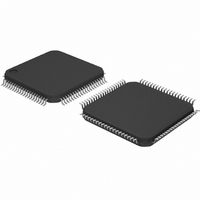
SC28L194A1BE,551 NXP Semiconductors, SC28L194A1BE,551 Datasheet - Page 29

SC28L194A1BE,551
Manufacturer Part Number
SC28L194A1BE,551
Description
IC UART QUAD W/FIFO 80-LQFP
Manufacturer
NXP Semiconductors
Datasheet
1.SC28L194A1BE528.pdf
(52 pages)
Specifications of SC28L194A1BE,551
Features
False-start Bit Detection
Number Of Channels
4, QUART
Fifo's
16 Byte
Voltage - Supply
3.3V, 5V
With Auto Flow Control
Yes
With False Start Bit Detection
Yes
With Modem Control
Yes
With Cmos
Yes
Mounting Type
Surface Mount
Package / Case
80-LQFP
Lead Free Status / RoHS Status
Lead free / RoHS Compliant
Other names
935262730551
SC28L194A1BE-S
SC28L194A1BE-S
SC28L194A1BE-S
SC28L194A1BE-S
Available stocks
Company
Part Number
Manufacturer
Quantity
Price
Company:
Part Number:
SC28L194A1BE,551
Manufacturer:
NXP Semiconductors
Quantity:
10 000
Philips Semiconductors
GENERAL PURPOSE OUTPUT PIN CONTROL
The following four registers control the function of the Gout0 and
Gout1 pins. These output pins have a unique control matrix which
includes a clocking mechanism that will allow the pin to change
synchronously with an internal or external stimulus. See diagram
below.
Table 39. GPOSR- General Purpose Output
GPOSR selects the signal or data source for the Gout pins. The Tx
and Rx clock selection is straight forward. The selection of the
GPOR allows a more flexible timing control of when the Gout pins
change.
Table 40. GPOR- General Purpose Output
This register is a read/write register. Its contents may be altered by a
GPOR Write or by the GPOC and GPOD registers shown below.
The GPOD and GPOC may be programmed to cause the individual
bits of the GPOR to change synchronously with internal or external
events. The cells of this register may be thought of as a “Two Port
flip-flop”; one port is controlled by a D input and clock, the other by a
data load strobe. A read of the GPOR always returns its current
value regardless of the port from which it was loaded.
2006 Aug 15
Global General Purpose Output
1
Selection
0000 - 0111 reserved
1000 = TxC1x a
1001 = TxC16x a
1010 = RxC16x a
1011 = TxC16x b
1100 = GGPOR(3)
1101 = GGPOR(2)
1110 = GGPOR(1)
1111 = GGPOR(0)
Reserved
Quad UART for 3.3 V and 5 V supply voltage
Bits 7:4
Select Register
Register
Bits 7:4
GPORQN
GPOR(3)
4:1 MULTIPLEX
4:1 MULTIPLEX
1/O3a
1/O3b
NONE
G
Bit 3
G
GPOD
IN
IN
“1”
“0”
GPOC
0
1
GPOR(2)
Bit 2
4
Global General Purpose Output
0
Selection
0000 - 0111 reserved
1000 = TxC1x a
1001 = TxC16x a
1010 = RxC16x a
1011 = TxC16x b
1100 = GGPOR(3)
1101 = GGPOR(2)
1110 = GGPOR(1)
1111 = GGPOR(0)
DATA BUS 3:0
GPOR R/W
4
GPOR(1)
Bit 1
Bits 3:0
Figure 3. General Purpose Pin Control Logic
DATA IN/OUT
DATA READ/WRITE
D INPUT
D CLOCK
GPOR
GPOR(0)
Bit 0
QN
29
RxC16Xa
TxC16Xa
TxC16Xb
4
TxC1Xa
Table 41. GPOC- General Purpose Output Clk
This controls the clock source for GPOR that will clock and/or toggle
the data from the selected GPOD source. When code b’00 is
selected, no clock will be provided, thereby preventing any change
through the D port.
Table 42. GPOD- General Purpose Output Data
This register selects the data that will be presented to the GPOR “D”
input. Note that selection b’10 selects the inverted GPOR data as
the input. In this case, the GPOR output will toggle synchronously
with the clock selected in the GPOC.
Clk Sel
GPOR(3)
00 = none
01 = GIN0
10 = GIN1
11 = reserved
Data Sel
GPOR(3)
00 = ’1’
01 = ’0’
10 = GPOR3N
11 = reserved
Bits 7:6
Bits 7:6
GPOR(0)
GPOR(1)
GPOR(2)
GPOR(3)
Register
Register
8:1 MULTIPLEX
GPOSR
Clk Sel
GPOR(2)
00 = none
01 = GIN0
10 = GIN1
11 = reserved
Data Sel
GPOR(2)
00 = ’1’
01 = ’0’
10 = GPOR2N
11 = reserved
Bits 5:4
Bits 5:4
Clk Sel
GPOR(1)
00 = none
01 = GIN0
10 = GIN1
11 = I/O3c
Data Sel
GPOR(1)
00 = ’1’
01 = ’0’
10 = GPOR1N
11 = I/O3d
Bits 3:2
Bits 3:2
SC28L194
GPO PIN
Product data sheet
SD00526
Clk Sel
GPOR(0)
00 = none
01 = GIN0
10 = GIN1
11 = I/O3a
Data Sel
GPOR(0)
00 = ’1’
01 = ’0’
10 = GPOR0N
11 = I/O3b
Bits 1:0
Bits 1:0


