SC28L92A1B,557 NXP Semiconductors, SC28L92A1B,557 Datasheet - Page 18
SC28L92A1B,557
Manufacturer Part Number
SC28L92A1B,557
Description
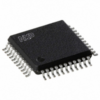
IC UART DUAL W/FIFO 44-PQFP
Manufacturer
NXP Semiconductors
Series
IMPACTr
Type
Dual UARTr
Datasheet
1.SC28L92A1B557.pdf
(73 pages)
Specifications of SC28L92A1B,557
Number Of Channels
2, DUART
Package / Case
44-MQFP, 44-PQFP
Features
False-start Bit Detection
Fifo's
16 Byte
Voltage - Supply
3.3V, 5V
With Auto Flow Control
Yes
With False Start Bit Detection
Yes
With Modem Control
Yes
With Cmos
Yes
Mounting Type
Surface Mount
Data Rate
0.2304 MBd
Supply Voltage (max)
3.63 V or 5.5 V
Supply Voltage (min)
2.97 V or 4.5 V
Supply Current
25 mA
Maximum Operating Temperature
+ 85 C
Minimum Operating Temperature
- 40 C
Mounting Style
SMD/SMT
Operating Supply Voltage
3.3 V or 5 V
Lead Free Status / RoHS Status
Lead free / RoHS Compliant
Lead Free Status / RoHS Status
Lead free / RoHS Compliant, Lead free / RoHS Compliant
Other names
568-1211
935263294557
SC28L92A1B
935263294557
SC28L92A1B
Available stocks
Company
Part Number
Manufacturer
Quantity
Price
Company:

Part Number:
SC28L92A1B,557
Manufacturer:
NXP Semiconductors
Quantity:
10 000


NXP Semiconductors
SC28L92_7
Product data sheet
6.2.10 Output port
6.3.1 Transmitter
6.3 Operation
The output ports are controlled from six places: the OPCR, OPR, MR, Command, SOPR
and ROPR registers. The OPCR register controls the source of the data for the output
ports OP2 through OP7. The data source for output ports OP0 and OP1 is controlled by
the MR and CR registers. When the OPR is the source of the data for the output ports, the
data at the ports is inverted from that in the OPR register. The content of the OPR register
is controlled by the set output port bits command and the reset output bits command.
These commands are at 0xE and 0xF, respectively. When these commands are used,
action takes place only at the bit locations where ones exist. For example, a one in bit
location 5 of the data word used with the set output port bits command will result in OPR5
being set to one. The OP5 would then be set to zero (V
of the data word associated with the reset output ports bits command would set OPR5 to
zero and, hence, the pin OP5 to a one (V
These pins along with the IP pins and their change-of-state detectors are often used for
modem and DMA control.
The SC28L92 is conditioned to transmit data when the transmitter is enabled through the
command register. The SC28L92 indicates to the CPU that it is ready to accept a
character by setting the TxRDY bit in the status register. This condition can be
programmed to generate an interrupt request at OP6 or OP7 and INTRN. When the
transmitter is initially enabled the TxRDY and TxEMPT bits will be set in the status
register. When a character is loaded to the transmit FIFO the TxEMPT bit will be reset.
The TxEMPT will not set until: 1) the transmit FIFO is empty and the transmit shift register
has finished transmitting the stop bit of the last character written to the transmit FIFO, or
2) the transmitter is disabled and then re-enabled. The TxRDY bit is set whenever the
transmitter is enabled and the Tx FIFO is not full. Data is transferred from the holding
register to transmit shift register when it is idle or has completed transmission of the
previous character. Characters cannot be loaded into the Tx FIFO while the transmitter is
disabled.
The transmitter converts the parallel data from the CPU to a serial bit stream on the TxD
output pin. It automatically sends a start bit followed by the programmed number of data
bits, an optional parity bit, and the programmed number of stop bits. The least significant
bit is sent first. Following the transmission of the stop bits, if a new character is not
available in the Tx FIFO, the TxD output remains HIGH and the TxEMT bit in the Status
Register (SR) will be set to 1. Transmission resumes and the TxEMT bit is cleared when
the CPU loads a new character into the Tx FIFO.
If the transmitter is disabled it continues operating until the character currently being
transmitted and any characters in the Tx FIFO, including parity and stop bits, have been
transmitted. New data cannot be loaded to the Tx FIFO when the transmitter is disabled.
When the transmitter is reset it stops sending data immediately.
The transmitter can be forced to send a break (a continuous LOW condition) by issuing a
START BREAK command via the CR register. The break is terminated by a STOP BREAK
command or a transmitter reset.
Rev. 07 — 19 December 2007
3.3 V/5.0 V Dual Universal Asynchronous Receiver/Transmitter
DD
).
SS
). Similarly, a one in bit position 5
SC28L92
© NXP B.V. 2007. All rights reserved.
18 of 73
Related parts for SC28L92A1B,557
Image
Part Number
Description
Manufacturer
Datasheet
Request
R

Part Number:
Description:
NXP Semiconductors designed the LPC2420/2460 microcontroller around a 16-bit/32-bitARM7TDMI-S CPU core with real-time debug interfaces that include both JTAG andembedded trace
Manufacturer:
NXP Semiconductors
Datasheet:

Part Number:
Description:
NXP Semiconductors designed the LPC2458 microcontroller around a 16-bit/32-bitARM7TDMI-S CPU core with real-time debug interfaces that include both JTAG andembedded trace
Manufacturer:
NXP Semiconductors
Datasheet:
Part Number:
Description:
NXP Semiconductors designed the LPC2468 microcontroller around a 16-bit/32-bitARM7TDMI-S CPU core with real-time debug interfaces that include both JTAG andembedded trace
Manufacturer:
NXP Semiconductors
Datasheet:
Part Number:
Description:
NXP Semiconductors designed the LPC2470 microcontroller, powered by theARM7TDMI-S core, to be a highly integrated microcontroller for a wide range ofapplications that require advanced communications and high quality graphic displays
Manufacturer:
NXP Semiconductors
Datasheet:
Part Number:
Description:
NXP Semiconductors designed the LPC2478 microcontroller, powered by theARM7TDMI-S core, to be a highly integrated microcontroller for a wide range ofapplications that require advanced communications and high quality graphic displays
Manufacturer:
NXP Semiconductors
Datasheet:
Part Number:
Description:
The Philips Semiconductors XA (eXtended Architecture) family of 16-bit single-chip microcontrollers is powerful enough to easily handle the requirements of high performance embedded applications, yet inexpensive enough to compete in the market for hi
Manufacturer:
NXP Semiconductors
Datasheet:
Part Number:
Description:
The XA-S3 device is a member of Philips Semiconductors? XA(eXtended Architecture) family of high performance 16-bitsingle-chip microcontrollers
Manufacturer:
NXP Semiconductors
Datasheet:

Part Number:
Description:
The NXP BlueStreak LH75401/LH75411 family consists of two low-cost 16/32-bit System-on-Chip (SoC) devices
Manufacturer:
NXP Semiconductors
Datasheet:
Part Number:
Description:
The NXP LPC3130/3131 combine an 180 MHz ARM926EJ-S CPU core, high-speed USB2
Manufacturer:
NXP Semiconductors
Datasheet:
Part Number:
Description:
The NXP LPC3141 combine a 270 MHz ARM926EJ-S CPU core, High-speed USB 2
Manufacturer:
NXP Semiconductors
Part Number:
Description:
The NXP LPC3143 combine a 270 MHz ARM926EJ-S CPU core, High-speed USB 2
Manufacturer:
NXP Semiconductors

Part Number:
Description:
The NXP LPC3152 combines an 180 MHz ARM926EJ-S CPU core, High-speed USB 2
Manufacturer:
NXP Semiconductors
Part Number:
Description:
The NXP LPC3154 combines an 180 MHz ARM926EJ-S CPU core, High-speed USB 2
Manufacturer:
NXP Semiconductors

Part Number:
Description:
Standard level N-channel enhancement mode Field-Effect Transistor (FET) in a plastic package using NXP High-Performance Automotive (HPA) TrenchMOS technology
Manufacturer:
NXP Semiconductors
Datasheet: