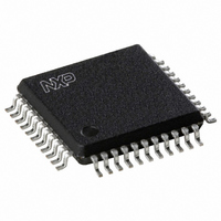
SC28L92A1B,557 NXP Semiconductors, SC28L92A1B,557 Datasheet - Page 17

SC28L92A1B,557
Manufacturer Part Number
SC28L92A1B,557
Description
IC UART DUAL W/FIFO 44-PQFP
Manufacturer
NXP Semiconductors
Series
IMPACTr
Type
Dual UARTr
Datasheet
1.SC28L92A1B557.pdf
(73 pages)
Specifications of SC28L92A1B,557
Number Of Channels
2, DUART
Package / Case
44-MQFP, 44-PQFP
Features
False-start Bit Detection
Fifo's
16 Byte
Voltage - Supply
3.3V, 5V
With Auto Flow Control
Yes
With False Start Bit Detection
Yes
With Modem Control
Yes
With Cmos
Yes
Mounting Type
Surface Mount
Data Rate
0.2304 MBd
Supply Voltage (max)
3.63 V or 5.5 V
Supply Voltage (min)
2.97 V or 4.5 V
Supply Current
25 mA
Maximum Operating Temperature
+ 85 C
Minimum Operating Temperature
- 40 C
Mounting Style
SMD/SMT
Operating Supply Voltage
3.3 V or 5 V
Lead Free Status / RoHS Status
Lead free / RoHS Compliant
Lead Free Status / RoHS Status
Lead free / RoHS Compliant, Lead free / RoHS Compliant
Other names
568-1211
935263294557
SC28L92A1B
935263294557
SC28L92A1B
Available stocks
Company
Part Number
Manufacturer
Quantity
Price
Company:
Part Number:
SC28L92A1B,557
Manufacturer:
NXP Semiconductors
Quantity:
10 000
NXP Semiconductors
SC28L92_7
Product data sheet
6.2.7 Time-out mode caution
6.2.8 Communications channels A and B
6.2.9 Input port
Counter/Timer upper register. These commands have slight differences depending on the
mode of operation. Please see the detail of the commands in
registers”.
When operating in the special time-out mode, it is possible to generate what appears to be
a false interrupt, i.e., an interrupt without a cause. This may result when a time-out
interrupt occurs and then, before the interrupt is serviced, another character is received,
i.e., the data stream has started again. (The interrupt latency is longer than the pause in
the data stream.) In this case, when a new character has been received, the counter/timer
will be restarted by the receiver, thereby withdrawing its interrupt. If, at this time, the
interrupt service begins for the previously seen interrupt, a read of the ISR will show the
Counter Ready bit not set. If nothing else is interrupting, this read of the ISR will return a
0x00 character. This action may present the appearance of a spurious interrupt.
Each communications channel of the SC28L92 comprises a full-duplex asynchronous
receiver/transmitter (UART). The operating frequency for each receiver and transmitter
can be selected independently from the baud rate generator, the counter/timer, or from an
external input. The transmitter accepts parallel data from the CPU, converts it to a serial
bit stream, inserts the appropriate start, stop, and optional parity bits and outputs a
composite serial stream of data on the TxD output pin. The receiver accepts serial data on
the RxD pin, converts this serial input to parallel format, checks for start bit, stop bit, parity
bit (if any), or break condition and sends an assembled character to the CPU via the
receive FIFO. Three status bits (break received, framing and parity errors) are also
FIFOed with each data character.
The inputs to this unlatched 7-bit (6-bit for 68xxx mode) port can be read by the CPU by
performing a read operation at address 0xD. A HIGH input results in a logic 1 while a LOW
input results in a logic 0. D7 will always read as a logic 1. The pins of this port can also
serve as auxiliary inputs to certain portions of the DUART logic, modem and DMA.
Four change-of-state detectors are provided which are associated with inputs IP3, IP2,
IP1 and IP0. A HIGH-to-LOW or LOW-to-HIGH transition of these inputs, lasting longer
than 25 s to 50 s, will set the corresponding bit in the input port change register. The
bits are cleared when the register is read by the CPU. Any change of state can also be
programmed to generate an interrupt to the CPU.
The input port change of state detection circuitry uses a 38.4 kHz sampling clock derived
from one of the baud rate generator taps. This results in a sampling period of slightly more
than 25 s (this assumes that the clock input is 3.6864 MHz). The detection circuitry, in
order to guarantee that a true change in level has occurred, requires two successive
samples at the new logic level be observed. As a consequence, the minimum duration of
the signal change is 25 s if the transition occurs coincident with the first sample pulse.
The 50 s time refers to the situation in which the change of state is just missed and the
first change of state is not detected until 25 s later.
Rev. 07 — 19 December 2007
3.3 V/5.0 V Dual Universal Asynchronous Receiver/Transmitter
Section 7.3.3 “Command
SC28L92
© NXP B.V. 2007. All rights reserved.
17 of 73


