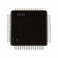
SC16C554BIBM,151 NXP Semiconductors, SC16C554BIBM,151 Datasheet - Page 20

SC16C554BIBM,151
Manufacturer Part Number
SC16C554BIBM,151
Description
IC UART QUAD W/FIFO 64-LQFP
Manufacturer
NXP Semiconductors
Datasheet
1.SC16C554BIBS551.pdf
(58 pages)
Specifications of SC16C554BIBM,151
Number Of Channels
4, QUART
Fifo's
16 Byte
Voltage - Supply
2.5V, 3.3V, 5V
With Auto Flow Control
Yes
With False Start Bit Detection
Yes
With Modem Control
Yes
With Cmos
Yes
Mounting Type
Surface Mount
Package / Case
64-LQFP
Lead Free Status / RoHS Status
Lead free / RoHS Compliant
Other names
568-3267
935279067151
SC16C554BIBM-S
935279067151
SC16C554BIBM-S
Available stocks
Company
Part Number
Manufacturer
Quantity
Price
Company:
Part Number:
SC16C554BIBM,151
Manufacturer:
NXP Semiconductors
Quantity:
10 000
NXP Semiconductors
SC16C554B_554DB
Product data sheet
Fig 12. RTS functional timing waveforms, RCV FIFO trigger level = 14 bytes
RTS
IOR
RX
(1) RTS is de-asserted when the receiver receives the first data bit of the sixteenth byte. The receive FIFO is full after finishing the
(2) RTS is asserted again when there is at least one byte of space available and no incoming byte is in processing, or there is more
(3) When the receive FIFO is full, the first receive buffer register read re-asserts RTS.
sixteenth byte.
than one byte of space available.
6.5 Hardware/software and time-out interrupts
6.6 Programmable baud rate generator
byte 14
Following a reset, if the transmitter interrupt is enabled, the SC16C554B/554DB will issue
an interrupt to indicate that the Transmit Holding Register is empty. This interrupt must be
serviced prior to continuing operations. The LSR register provides the current singular
highest priority interrupt only. Only after servicing the higher pending interrupt will the
lower priority interrupt(s) be reflected in the status register. Servicing the interrupt without
investigating further interrupt conditions can result in data errors.
When two interrupt conditions have the same priority, it is important to service these
interrupts correctly. Receive Data Ready and Receive Time-Out have the same interrupt
priority (when enabled by IER[0]). The receiver issues an interrupt after the number of
characters have reached the programmed trigger level. In this case, the
SC16C554B/554DB FIFO may hold more characters than the programmed trigger level.
Following the removal of a data byte, the user should re-check LSR[0] for additional
characters. A Receive Time-Out will not occur if the receive FIFO is empty. The time-out
counter is reset at the center of each stop bit received or each time the Receive Holding
Register (RHR) is read. The actual time-out value is 4 character time.
In the 16 mode for the PLCC68 package, the system/board designer can optionally
provide software controlled 3-state interrupt operation. This is accomplished by INTSEL
and MCR[3]. When INTSEL interface pin is left open or made a logic 0, MCR[3] controls
the 3-state interrupt outputs, INTA to INTD. When INTSEL is a logic 1, MCR[3] has no
effect on the INTA to INTD outputs, and the package operates with interrupt outputs
enabled continuously.
The SC16C554B/554DB supports high speed modem technologies that have increased
input data rates by employing data compression schemes. For example, a 33.6 kbit/s
modem that employs data compression may require a 115.2 kbit/s input data rate.
A 128.0 kbit/s ISDN modem that supports data compression may need an input data rate
of 460.8 kbit/s.
RTS released after the
first data bit of byte 16
byte 15
All information provided in this document is subject to legal disclaimers.
5 V, 3.3 V and 2.5 V quad UART, 5 Mbit/s (max.) with 16-byte FIFOs
Rev. 4 — 8 June 2010
Start
byte 16
Stop
SC16C554B/554DB
Start
byte 18
© NXP B.V. 2010. All rights reserved.
Stop
002aaa051
20 of 58


