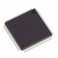
DS21552L+ Maxim Integrated Products, DS21552L+ Datasheet - Page 54

DS21552L+
Manufacturer Part Number
DS21552L+
Description
IC TXRX T1 1-CHIP 5V 100-LQFP
Manufacturer
Maxim Integrated Products
Datasheet
1.DS21352L.pdf
(137 pages)
Specifications of DS21552L+
Function
Single-Chip Transceiver
Interface
E1, HDLC, J1, T1
Number Of Circuits
1
Voltage - Supply
4.75 V ~ 5.25 V
Current - Supply
75mA
Operating Temperature
0°C ~ 70°C
Mounting Type
Surface Mount
Package / Case
100-LQFP
Includes
DSX-1 and CSU Line Build-Out Generator, HDLC Controller, In-Band Loop Code Generator and Detector
Product
Framer
Number Of Transceivers
1
Data Rate
64 Kbps
Supply Voltage (max)
3.465 V
Supply Voltage (min)
3.135 V
Supply Current (max)
75 mA (Typ)
Maximum Operating Temperature
+ 70 C
Minimum Operating Temperature
0 C
Mounting Style
SMD/SMT
Ic Interface Type
Parallel, Serial
Supply Voltage Range
4.75V To 5.25V
Operating Temperature Range
0°C To +70°C
Digital Ic Case Style
LQFP
No. Of Pins
100
Filter Terminals
SMD
Rohs Compliant
Yes
Lead Free Status / RoHS Status
Lead free / RoHS Compliant
Power (watts)
-
Lead Free Status / Rohs Status
Lead free / RoHS Compliant
9. DS0 MONITORING FUNCTION
The device has the ability to monitor one DS0 64kbps channel in the transmit direction and one DS0
channel in the receive direction at the same time. In the transmit direction the user will determine which
channel is to be monitored by properly setting the TCM0 to TCM4 bits in the CCR5 register. In the
receive direction, the RCM0 to RCM4 bits in the CCR6 register need to be properly set. The DS0 channel
pointed to by the TCM0 to TCM4 bits will appear in the Transmit DS0 Monitor (TDS0M) register and
the DS0 channel pointed to by the RCM0 to RCM4 bits will appear in the Receive DS0 (RDS0M)
register. The TCM4 to TCM0 and RCM4 to RCM0 bits should be programmed with the decimal decode
of the appropriate T1 channel. For example, if DS0 channel 6 in the transmit direction and DS0 channel
15 in the receive direction needed to be monitored, then the following values would be programmed into
CCR5 and CCR6:
CCR5: COMMON CONTROL REGISTER 5 (Address=19 Hex)
[repeated here from section 6 for convenience]
SYMBOL
(MSB)
TCM4
TCM3
TCM2
TCM1
TCM0
TJC
LIAIS
LLB
TJC
TCM4 = 0
TCM3 = 0
TCM2 = 1
TCM1 = 0
TCM0 = 1
POSITION
LLB
CCR5.7
CCR5.6
CCR5.5
CCR5.4
CCR5.3
CCR5.2
CCR5.1
CCR5.0
RCM4 = 0
RCM3 = 1
RCM2 = 1
RCM1 = 1
RCM0 = 0
LIAIS
NAME AND DESCRIPTION
Transmit Japanese CRC6 Enable.
Local Loopback.
Line Interface AIS Generation Enable.
Transmit Channel Monitor Bit 4. MSB of a channel decode that determines which
transmit channel data will appear in the TDS0M register. See Section 0 for details.
Transmit Channel Monitor Bit 3.
Transmit Channel Monitor Bit 2.
Transmit Channel Monitor Bit 1.
Transmit Channel Monitor Bit 0. LSB of the channel decode.
TCM4
54 of 137
TCM3
TCM2
TCM1
TCM0
(LSB)


