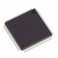
DS21552L+ Maxim Integrated Products, DS21552L+ Datasheet - Page 104

DS21552L+
Manufacturer Part Number
DS21552L+
Description
IC TXRX T1 1-CHIP 5V 100-LQFP
Manufacturer
Maxim Integrated Products
Datasheet
1.DS21352L.pdf
(137 pages)
Specifications of DS21552L+
Function
Single-Chip Transceiver
Interface
E1, HDLC, J1, T1
Number Of Circuits
1
Voltage - Supply
4.75 V ~ 5.25 V
Current - Supply
75mA
Operating Temperature
0°C ~ 70°C
Mounting Type
Surface Mount
Package / Case
100-LQFP
Includes
DSX-1 and CSU Line Build-Out Generator, HDLC Controller, In-Band Loop Code Generator and Detector
Product
Framer
Number Of Transceivers
1
Data Rate
64 Kbps
Supply Voltage (max)
3.465 V
Supply Voltage (min)
3.135 V
Supply Current (max)
75 mA (Typ)
Maximum Operating Temperature
+ 70 C
Minimum Operating Temperature
0 C
Mounting Style
SMD/SMT
Ic Interface Type
Parallel, Serial
Supply Voltage Range
4.75V To 5.25V
Operating Temperature Range
0°C To +70°C
Digital Ic Case Style
LQFP
No. Of Pins
100
Filter Terminals
SMD
Rohs Compliant
Yes
Lead Free Status / RoHS Status
Lead free / RoHS Compliant
Power (watts)
-
Lead Free Status / Rohs Status
Lead free / RoHS Compliant
- Current page: 104 of 137
- Download datasheet (2Mb)
IDENTIFICATION REGISTER
The identification register contains a 32-bit shift register and a 32-bit latched parallel output. This
register is selected during the IDCODE instruction and when the TAP controller is in the Test-Logic-
Reset state. See Table 19-2. Table 19-3 lists the device ID codes for the SCT devices.
Table 19-4 BOUNDARY SCAN CONTROL BITS
Table 19-4 BOUNDARY SCAN CONTROL BITS (cont.)
BIT
BIT
72
71
70
69
68
67
66
65
64
63
62
61
60
59
58
57
56
55
54
2
1
0
PIN
PIN
10
11
12
13
14
15
16
17
18
19
20
21
22
23
24
25
26
27
28
29
30
31
32
33
34
35
36
37
38
39
40
41
42
43
44
1
2
3
4
5
6
7
8
9
–
TSYNC.cntl
SYMBOL
SYMBOL
RCHBLK
TCHBLK
8MCLK
XTALD
TNEGO
TSYNC
TCLKO
8XCLK
TLCLK
TPOSO
RRING
TRING
TNEGI
JTCLK
TLINK
TCLKI
JTRST
RVDD
MCLK
DVDD
TVDD
TPOSI
RVSS
RVSS
RVSS
JTMS
JTDO
TEST
TVSS
LIUC
RTIP
TTIP
JTDI
RCL
BTS
INT
N/C
N/C
N/C
N/C
N/C
NC
NC
CI
TYPE
TYPE
104 of 137
I/O
O
O
O
O
O
O
O
O
O
O
O
O
O
O
–
–
–
–
–
–
–
–
–
–
–
–
–
–
–
I
I
I
I
I
I
I
I
I
I
I
I
I
I
I
1 = TSYNC an output
0 = TSYNC an input
CONTROL BIT DESCRIPTION
CONTROL BIT DESCRIPTION
Related parts for DS21552L+
Image
Part Number
Description
Manufacturer
Datasheet
Request
R

Part Number:
Description:
Manufacturer:
Maxim Integrated Products
Datasheet:

Part Number:
Description:
Ds2155 T1/e1/j1 Single-chip Transceiver
Manufacturer:
Maxim Integrated Products, Inc.
Datasheet:

Part Number:
Description:
MAX7528KCWPMaxim Integrated Products [CMOS Dual 8-Bit Buffered Multiplying DACs]
Manufacturer:
Maxim Integrated Products
Datasheet:

Part Number:
Description:
Single +5V, fully integrated, 1.25Gbps laser diode driver.
Manufacturer:
Maxim Integrated Products
Datasheet:

Part Number:
Description:
Single +5V, fully integrated, 155Mbps laser diode driver.
Manufacturer:
Maxim Integrated Products
Datasheet:

Part Number:
Description:
VRD11/VRD10, K8 Rev F 2/3/4-Phase PWM Controllers with Integrated Dual MOSFET Drivers
Manufacturer:
Maxim Integrated Products
Datasheet:

Part Number:
Description:
Highly Integrated Level 2 SMBus Battery Chargers
Manufacturer:
Maxim Integrated Products
Datasheet:

Part Number:
Description:
Current Monitor and Accumulator with Integrated Sense Resistor; ; Temperature Range: -40°C to +85°C
Manufacturer:
Maxim Integrated Products

Part Number:
Description:
TSSOP 14/A°/RS-485 Transceivers with Integrated 100O/120O Termination Resis
Manufacturer:
Maxim Integrated Products

Part Number:
Description:
TSSOP 14/A°/RS-485 Transceivers with Integrated 100O/120O Termination Resis
Manufacturer:
Maxim Integrated Products

Part Number:
Description:
QFN 16/A°/AC-DC and DC-DC Peak-Current-Mode Converters with Integrated Step
Manufacturer:
Maxim Integrated Products

Part Number:
Description:
TDFN/A/65V, 1A, 600KHZ, SYNCHRONOUS STEP-DOWN REGULATOR WITH INTEGRATED SWI
Manufacturer:
Maxim Integrated Products

Part Number:
Description:
Integrated Temperature Controller f
Manufacturer:
Maxim Integrated Products

Part Number:
Description:
SOT23-6/I°/45MHz to 650MHz, Integrated IF VCOs with Differential Output
Manufacturer:
Maxim Integrated Products

Part Number:
Description:
SOT23-6/I°/45MHz to 650MHz, Integrated IF VCOs with Differential Output
Manufacturer:
Maxim Integrated Products


