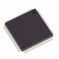
DS21352L+ Maxim Integrated Products, DS21352L+ Datasheet - Page 36

DS21352L+
Manufacturer Part Number
DS21352L+
Description
IC TXRX T1 1-CHIP 3.3V 100-LQFP
Manufacturer
Maxim Integrated Products
Datasheet
1.DS21352L.pdf
(137 pages)
Specifications of DS21352L+
Function
Single-Chip Transceiver
Interface
HDLC, T1
Number Of Circuits
1
Voltage - Supply
3.14 V ~ 3.47 V
Current - Supply
75mA
Operating Temperature
0°C ~ 70°C
Mounting Type
Surface Mount
Package / Case
100-LQFP
Includes
DSX-1 and CSU Line Build-Out Generator, HDLC Controller, In-Band Loop Code Generator and Detector
Lead Free Status / RoHS Status
Lead free / RoHS Compliant
Power (watts)
-
- Current page: 36 of 137
- Download datasheet (2Mb)
3. All receive side signals will take on timing synchronous with TCLK instead of RCLKI.
Please note that it is not acceptable to have RCLK tied to TCLK during this loopback because this
will cause an unstable condition.
CCR2: COMMON CONTROL REGISTER 2 (Address=38 Hex)
CCR3: COMMON CONTROL REGISTER 3 (Address=30 Hex)
RESMDM
TCLKSRC
SYMBOL
SYMBOL
RESMDM
(MSB)
(MSB)
TSLC96
RSLC96
RLOSF
TFM
TB8ZS
RB8ZS
TFDL
RZSE
TFM
RFM
TCLKSRC
TB8ZS
POSITION
POSITION
CCR2.7
CCR2.6
CCR2.5
CCR2.4
CCR2.3
CCR2.2
CCR2.1
CCR2.0
CCR3.7
CCR3.6
CCR3.5
TSLC96
RLOSF
NAME AND DESCRIPTION
Transmit Frame Mode Select.
0 = D4 framing mode
1 = ESF framing mode
Transmit B8ZS Enable.
0 = B8ZS disabled
1 = B8ZS enabled
Transmit SLC–96 / Fs–Bit Insertion Enable. Only set this bit to a one in D4 framing
applications. Must be set to one to source the Fs pattern from the TFDL register. See
Section 15.5 for details.
0 = SLC–96/Fs–bit insertion disabled
1 = SLC–96/Fs–bit insertion enabled
Transmit FDL Zero Stuffer Enable. Set this bit to zero if using the internal
HDLC/BOC controller instead of the legacy support for the FDL. See Section 15 for
details.
0 = zero stuffer disabled
1 = zero stuffer enabled
Receive Frame Mode Select.
0 = D4 framing mode
1 = ESF framing mode
Receive B8ZS Enable.
0 = B8ZS disabled
1 = B8ZS enabled
Receive SLC–96 Enable. Only set this bit to a one in D4/SLC–96 framing
applications. See Section 15.5 for details.
0 = SLC–96 disabled
1 = SLC–96 enabled
Receive FDL Zero Destuffer Enable. Set this bit to zero if using the internal
HDLC/BOC controller instead of the legacy support for the FDL. See Section 15.4 for
details.
0 = zero destuffer disabled
1 = zero destuffer enabled
NAME AND DESCRIPTION
Receive Elastic Store Minimum Delay Mode. See Section 14.4 for details.
0 = elastic stores operate at full two frame depth
1 = elastic stores operate at 32–bit depth
Transmit Clock Source Select. This function allows the user to internally select
RCLK as the clock source for the transmit side formatter.
0 = Source of transmit clock determined by TCR1.7 (LOTCMC)
1 = Force transmitter to internally switch to RCLK as source of transmit clock. Signal
at TCLK pin is ignored
Function of the RLOS/LOTC Output.
0 = Receive Loss of Sync (RLOS)
TFDL
RSMS
36 of 137
RFM
PDE
RB8ZS
ECUS
RSLC96
TLOOP
TESMDM
(LSB)
(LSB)
RZSE
Related parts for DS21352L+
Image
Part Number
Description
Manufacturer
Datasheet
Request
R

Part Number:
Description:
MAX7528KCWPMaxim Integrated Products [CMOS Dual 8-Bit Buffered Multiplying DACs]
Manufacturer:
Maxim Integrated Products
Datasheet:

Part Number:
Description:
Single +5V, fully integrated, 1.25Gbps laser diode driver.
Manufacturer:
Maxim Integrated Products
Datasheet:

Part Number:
Description:
Single +5V, fully integrated, 155Mbps laser diode driver.
Manufacturer:
Maxim Integrated Products
Datasheet:

Part Number:
Description:
VRD11/VRD10, K8 Rev F 2/3/4-Phase PWM Controllers with Integrated Dual MOSFET Drivers
Manufacturer:
Maxim Integrated Products
Datasheet:

Part Number:
Description:
Highly Integrated Level 2 SMBus Battery Chargers
Manufacturer:
Maxim Integrated Products
Datasheet:

Part Number:
Description:
Current Monitor and Accumulator with Integrated Sense Resistor; ; Temperature Range: -40°C to +85°C
Manufacturer:
Maxim Integrated Products

Part Number:
Description:
TSSOP 14/A�/RS-485 Transceivers with Integrated 100O/120O Termination Resis
Manufacturer:
Maxim Integrated Products

Part Number:
Description:
TSSOP 14/A�/RS-485 Transceivers with Integrated 100O/120O Termination Resis
Manufacturer:
Maxim Integrated Products

Part Number:
Description:
QFN 16/A�/AC-DC and DC-DC Peak-Current-Mode Converters with Integrated Step
Manufacturer:
Maxim Integrated Products

Part Number:
Description:
TDFN/A/65V, 1A, 600KHZ, SYNCHRONOUS STEP-DOWN REGULATOR WITH INTEGRATED SWI
Manufacturer:
Maxim Integrated Products

Part Number:
Description:
Integrated Temperature Controller f
Manufacturer:
Maxim Integrated Products

Part Number:
Description:
SOT23-6/I�/45MHz to 650MHz, Integrated IF VCOs with Differential Output
Manufacturer:
Maxim Integrated Products

Part Number:
Description:
SOT23-6/I�/45MHz to 650MHz, Integrated IF VCOs with Differential Output
Manufacturer:
Maxim Integrated Products

Part Number:
Description:
EVALUATION KIT/2.4GHZ TO 2.5GHZ 802.11G/B RF TRANSCEIVER WITH INTEGRATED PA
Manufacturer:
Maxim Integrated Products

Part Number:
Description:
QFN/E/DUAL PCIE/SATA HIGH SPEED SWITCH WITH INTEGRATED BIAS RESISTOR
Manufacturer:
Maxim Integrated Products
Datasheet:


