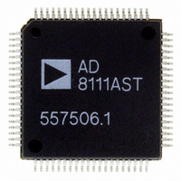
AD8111AST Analog Devices Inc, AD8111AST Datasheet

AD8111AST
Specifications of AD8111AST
Available stocks
Related parts for AD8111AST
AD8111AST Summary of contents
Page 1
PRODUCT DESCRIPTION The AD8110 and AD8111 are high-speed 16 × 8 video cross- point switch matrices. They offer a –3 dB signal bandwidth greater than 260 MHz, and channel switch times of less than 25 ns with 1% settling. ...
Page 2
AD8110/AD8111–SPECIFICATIONS Parameter DYNAMIC PERFORMANCE –3 dB Bandwidth Propagation Delay Slew Rate Settling Time Gain Flatness NOISE/DISTORTION PERFORMANCE Differential Gain Error Differential Phase Error Crosstalk, All Hostile Off Isolation, Input-Output Input Voltage Noise DC PERFORMANCE Gain Error Gain Matching Gain Temperature ...
Page 3
TIMING CHARACTERISTICS (Serial) Parameter Serial Data Setup Time CLK Pulsewidth Serial Data Hold Time CLK Pulse Separation, Serial Mode CLK to UPDATE Delay UPDATE Pulsewidth CLK to DATA OUT Valid, Serial Mode Propagation Delay, UPDATE to Switch On or Off ...
Page 4
AD8110/AD8111 TIMING CHARACTERISTICS (Parallel) Parameter Data Setup Time CLK Pulsewidth Data Hold Time CLK Pulse Separation CLK to UPDATE Delay UPDATE Pulsewidth Propagation Delay, UPDATE to Switch On or Off CLK, UPDATE Rise and Fall Times RESET Time 1 CLK ...
Page 5
... Temperature Model Range AD8110AST –40°C to +85°C AD8111AST –40°C to +85°C AD8110-EB AD8111-EB CAUTION ESD (electrostatic discharge) sensitive device. Electrostatic charges as high as 4000 V readily accumulate on the human body and test equipment and can discharge without detection. Although the AD8110/AD8111 features proprietary ESD protection circuitry, permanent damage may occur on devices subjected to high-energy electrostatic discharges ...
Page 6
AD8110/AD8111 CE UPDATE CLK DATA Data D4 PARALLEL D1 DATA ...
Page 7
Pin Name Pin Numbers INxx 66, 68, 70, 72, 74, 76, 78 11, 13, 15, 64 DATA IN 57 CLK 58 DATA OUT 59 UPDATE 56 RESET SER/PAR 55 OUTyy 41, 38, ...
Page 8
AD8110/AD8111 IN08 1 AGND 2 IN09 3 AGND 4 IN10 5 AGND 6 IN11 7 AGND 8 9 IN12 AGND 10 IN13 11 AGND 12 IN14 13 AGND 14 IN15 15 AGND 16 AVEE 17 AVCC 18 AVCC07 19 20 ...
Page 9
Typical Performance Characteristics–AD8110/AD8111 150 FLATNESS 1 0 GAIN –1 2V p-p –2 –3 100k 1M 10M 100M FREQUENCY – Hz – –40 –50 –60 ALL HOSTILE –70 ADJACENT –80 ...
Page 10
AD8110/AD8111 FLATNESS 1 0 GAIN –1 2V p-p –2 –3 100k 1M 10M FREQUENCY – Hz – –30 –40 –50 ADJACENT –60 –70 –80 ALL HOSTILE –90 –100 –110 0 ...
Page 11
R = 150 10k 100k 1M FREQUENCY Hz 100 56.3 31.6 17 5.63 3.16 10 100 1k 10k 100k FREQUENCY Hz 1M 100k 10k 1k 100 0 FREQUENCY ...
Page 12
AD8110/AD8111 – 150 L –40 –50 –60 –70 –80 10k 100k FREQUENCY – Hz 100 56.3 31.6 17.8 10 5.63 3.16 10 100 1k 10k FREQUENCY 100k 10k 1k 100 10 0 FREQUENCY 1M 10M –40 ...
Page 13
FREQUENCY – 200mV p 150 18pF = 7.7dB 6 4 12pF = 4.5dB 2 0 –2 –4 0.1M 1M ...
Page 14
AD8110/AD8111 10M 1M 100k 10k 1k 100 30k 100k 1M 10M FREQUENCY – –2 –4 –6 0.1M 1M 10M FREQUENCY – 100mV IN 0 150 L ...
Page 15
THEORY OF OPERATION The AD8110 (G = +1) and AD8111 (G = +2) share a common core architecture consisting of an array of 128 transconductance (gm) input stages organized as eight 16:1 multiplexers with a common, 16-line analog input bus. ...
Page 16
AD8110/AD8111 This will ensure that the programming matrix is always in a known state. From then on, parallel programming can be used to modify a single output or more at a time similar fashion, if both CE and ...
Page 17
The basic concept in constructing larger crosspoint arrays is to connect inputs in parallel in a horizontal direction and to “wire-OR” the outputs together in the vertical direction. The meaning of horizontal and vertical can best be understood by looking ...
Page 18
AD8110/AD8111 Multichannel Video The excellent video specifications of the AD8110/AD8111 make them ideal candidates for creating composite video crosspoint switches. These can be made quite dense by taking advantage of the AD8110/AD8111’s high level of integration and the fact that ...
Page 19
Measuring Crosstalk Crosstalk is measured by applying a signal to one or more channels and measuring the relative strength of that signal on a desired selected channel. The measurement is usually expressed as dB down from the magnitude of the ...
Page 20
AD8110/AD8111 From a circuit standpoint, this output crosstalk mechanism looks like a transformer with a mutual inductance between the windings that drives a load resistor. For low frequencies, the magnitude of the crosstalk is given by × XT ...
Page 21
DVCC DGND NC AVEE AGND AVCC NC P1-7 P1-1 P1-2 P1-3 P1-4 P1-5 P1 CR1 CR2 + INPUT 00 INPUT 00 65 AGND 75 66 ...
Page 22
AD8110/AD8111 ...
Page 23
AD8110/AD8111 ...
Page 24
AD8110/AD8111 The three power supply pins AVCC, DVCC, and AVEE should be connected to good quality, low noise, ± supplies. Where the same ± power supplies are used for analog and digital, separate cables should be ...
Page 25
Figure 16 shows the main screen of the control software in its initial reset state (all outputs off). Using the mouse, any input can be connected with one or more outputs by simply clicking on the appropriate radio buttons in ...
Page 26
AD8110/AD8111 0.030 (0.75) 0.020 (0.50) OUTLINE DIMENSIONS Dimensions shown in inches and (mm). 80-Lead Plastic LQFP (ST-80A) 0.559 (14.20) 0.063 (1.60) 0.543 (13.80) MAX 0.476 (12.10) 0.469 (11.90 SEATING PLANE TOP VIEW (PINS DOWN) 0.003 (0.08 ...
Page 27
Revision History Location Data Sheet changed from REV REV. A. Universal change in nomenclature from MQFP to LQFP Comment added to OUTLINE DIMENSIONS . . . . . . . . . . . . . . . ...
Page 28
...


