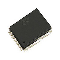
CY7C1351F-117AC Cypress Semiconductor Corp, CY7C1351F-117AC Datasheet - Page 4

CY7C1351F-117AC
Manufacturer Part Number
CY7C1351F-117AC
Description
Manufacturer
Cypress Semiconductor Corp
Datasheet
1.CY7C1351F-117AC.pdf
(15 pages)
Specifications of CY7C1351F-117AC
Density
4.5Mb
Access Time (max)
7.5ns
Sync/async
Synchronous
Architecture
SDR
Clock Freq (max)
117MHz
Operating Supply Voltage (typ)
3.3V
Address Bus
17b
Package Type
TQFP
Operating Temp Range
0C to 70C
Number Of Ports
1
Supply Current
220mA
Operating Supply Voltage (min)
3.135V
Operating Supply Voltage (max)
3.6V
Operating Temperature Classification
Commercial
Mounting
Surface Mount
Pin Count
100
Word Size
36b
Number Of Words
128K
Lead Free Status / Rohs Status
Not Compliant
Document #: 38-05210 Rev. *B
Pin Definitions
CE
OE
CEN
ZZ
DQ
DQP
MODE
V
V
V
NC
DD
DDQ
SS
3
Name
s
[A:D]
52,53,56,57,58,
59,62,63,68,69,
72,73,74,75,78,
12,13,18,19,22,
40,55,60,67,71,
14,16,38,39,42,
23,24,25,28,29
79,2,3,6,7,8,9,
5,10,17,21,26,
4,11,20,27,54,
15,41,65,91
43,66,83,84
51,80,1,30
61,70,77
76,90,
TQFP
92
86
87
64
31
D7,E7,G7,H7,
D1,E1,G1,H1,
K6,L6,M6,N6,
E6,F6,G6,H6,
E2,F2,G2,H2,
D4,G4,L4,U4,
K7,L7,N7,P7,
K1,L1,N1,P1,
A1,F1,J1,M1,
D3,E3,F3,H3,
J3,K3,M3,N3,
P3,D5,E5,F5,
H5,J5,K5,M5,
B1,C1,R1,T1,
T2,U2,U3,A4,
U5,T6,U6,B7,
K2,L2,M2,N2
P6,D6,D2,P2
U1,A7,F7,J7,
C7,R5,R7,T7
J2,C4,J4,R4,
M7,U7
N5,P5
BGA
M4
B6
R3
F4
T7
J6
I/O Power Sup-
Asynchronous
Asynchronous
Power Supply Power supply inputs to the core of the device.
Synchronous
Synchronous
Synchronous
Synchronous
Strap Pin
Ground
Input-
Input-
Input-
Input-
Input
I/O-
I/O-
I/O
ply
–
Chip Enable 3 Input, active LOW. Sampled on the rising edge
of CLK. Used in conjunction with CE
the device.
Output Enable, asynchronous input, active LOW. Combined
with the synchronous logic block inside the device to control the
direction of the I/O pins. When LOW, the I/O pins are allowed
to behave as outputs. When deasserted HIGH, I/O pins are
three-stated, and act as input data pins. OE is masked during
the data portion of a write sequence, during the first clock when
emerging from a deselected state, when the device has been
deselected.
Clock Enable Input, active LOW. When asserted LOW the
Clock signal is recognized by the SRAM. When deasserted
HIGH the Clock signal is masked. Since deasserting CEN does
not deselect the device, CEN can be used to extend the previ-
ous cycle when required.
ZZ “sleep” Input. This active HIGH input places the device in
a non-time critical “sleep” condition with data integrity pre-
served. During normal operation, this pin can be connected to
Vss or left floating.
Bidirectional Data I/O Lines. As inputs, they feed into an
on-chip data register that is triggered by the rising edge of CLK.
As outputs, they deliver the data contained in the memory loca-
tion specified by address during the clock rise of the read cycle.
The direction of the pins is controlled by OE and the internal
control logic. When OE is asserted LOW, the pins can behave
as outputs. When HIGH, DQ
three-state condition. The outputs are automatically three-stat-
ed during the data portion of a write sequence, during the first
clock when emerging from a deselected state, and when the
device is deselected, regardless of the state of OE.
Bidirectional Data Parity I/O Lines. Functionally, these signals
are identical to DQ
trolled by BW
Mode Input. Selects the burst order of the device.
When tied to Gnd selects linear burst sequence. When tied to
V
Power supply for the I/O circuitry.
Ground for the device.
No Connects. Not Internally connected to the die.
DD
or left floating selects interleaved burst sequence.
[A:D]
correspondingly.
s
. During write sequences, DQP
Description
s
and DQP
1
and CE
[A:D]
CY7C1351F
2
are placed in a
to select/deselect
Page 4 of 15
[A:D]
is con-
[+] Feedback


