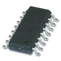
ADM3052BRWZ Analog Devices Inc, ADM3052BRWZ Datasheet - Page 14

ADM3052BRWZ
Manufacturer Part Number
ADM3052BRWZ
Description
58T4518
Manufacturer
Analog Devices Inc
Specifications of ADM3052BRWZ
Interface Type
CAN
No. Of Rx Buffers
1
Digital Ic Case Style
SOIC
No. Of Pins
16
Operating Temperature Range
-40°C To +85°C
Rohs Compliant
Yes
Number Of Transmitters
1
Power Supply Requirement
Dual
Operating Temperature Classification
Industrial
Mounting
Surface Mount
Operating Temperature (max)
85C
Operating Temperature (min)
-40C
Lead Free Status / Rohs Status
Compliant
Available stocks
Company
Part Number
Manufacturer
Quantity
Price
Company:
Part Number:
ADM3052BRWZ
Manufacturer:
ADI
Quantity:
68
Part Number:
ADM3052BRWZ
Manufacturer:
ADI/亚德诺
Quantity:
20 000
Part Number:
ADM3052BRWZ-REEL7
Manufacturer:
ADI/亚德诺
Quantity:
20 000
ADM3052
CIRCUIT DESCRIPTION
CAN TRANSCEIVER OPERATION
A CAN bus has two states: dominant and recessive. A dominant
state is present on the bus when the differential voltage between
CANH and CANL is greater than 0.9 V. A recessive state is
present on the bus when the differential voltage between CANH
and CANL is less than 0.5 V. During a dominant bus state, the
CANH pin is high and the CANL pin is low. During a recessive
bus state, both the CANH and CANL pins are in the high
impedance state.
ELECTRICAL ISOLATION
In the ADM3052, electrical isolation is implemented on the
logic side of the interface. Therefore, the part has two main
sections: a digital isolation section and a transceiver section
(see Figure 30). The driver input signal, which is applied to the
TxD pin and referenced to the logic ground (GND
across an isolation barrier to appear at the transceiver section
referenced to the isolated ground (V
input and V
the transceiver section, are coupled across the isolation barrier
to appear at the RxD pin and V
ground, respectively.
iCoupler Technology
The digital signals transmit across the isolation barrier using
iCoupler technology. This technique uses chip scale transformer
windings to couple the digital signals magnetically from one
side of the barrier to the other. Digital inputs are encoded into
waveforms that are capable of exciting the primary transformer
winding. At the secondary winding, the induced waveforms are
decoded into the binary value that was originally transmitted.
Positive and negative logic transitions at the input cause narrow
(~1 ns) pulses to be sent to the decoder via the transformer. The
decoder is bistable and is, therefore, set or reset by the pulses,
indicating input logic transitions. In the absence of logic transi-
tions at the input for more than ~1 μs, a periodic set of refresh
pulses, indicative of the correct input state, is sent to ensure dc
correctness at the output. If the decoder receives no internal
pulses for more than about 5 μs, the input side is assumed to be
unpowered or nonfunctional, in which case the output is forced
to a default state (see Table 9 and Table 10).
+
, which are referenced to the isolated ground in
+SENSE
−
referenced to the logic
). Similarly, the receiver
1
), is coupled
Rev. 0 | Page 14 of 20
TRUTH TABLES
The truth tables in this section use the abbreviations shown
in Table 8.
Table 8. Truth Table Abbreviations
Letter
H
L
I
X
Z
NC
Table 9. Transmitting
V
On
On
On
Off
On
Table 10. Receiving
Supply Status
V
On
On
On
On
Off
On
Supply Status Input
DD1
DD1
V
On
On
On
On
Off
V
On
On
On
On
On
Off
+
+
TxD
L
H
Floating
X
L
V
≥ 0.9 V
≤ 0.5 V
0.5 V < V
Inputs open
X
X
ID
= CANH − CANL
Description
High level
Low level
Indeterminate
Don’t care
High impedance (off)
Disconnected
ID
< 0.9 V
Bus State
Dominant
Recessive
Recessive
Recessive
I
Inputs
Bus State
Dominant
Recessive
I
Recessive
X
X
CANH
H
Z
Z
Z
I
Outputs
CANL
L
Z
Z
Z
I
RxD
L
H
I
H
I
H
Outputs
V
L
L
L
I
H
V
L
L
L
L
I
H
+SENSE
+SENSE


