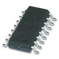
ADM3052BRWZ Analog Devices Inc, ADM3052BRWZ Datasheet

ADM3052BRWZ
Specifications of ADM3052BRWZ
Available stocks
Related parts for ADM3052BRWZ
ADM3052BRWZ Summary of contents
Page 1
FEATURES 5 kV rms isolated CAN transceiver Integrated V linear regulator + Bus side powered by V and V + − operation 3.3 V operation on V DD1 Complies ...
Page 2
ADM3052 TABLE OF CONTENTS Features .............................................................................................. 1 Applications ....................................................................................... 1 General Description ......................................................................... 1 Functional Block Diagram .............................................................. 1 Revision History ............................................................................... 2 Specifications ..................................................................................... 3 Timing Specifications .................................................................. 4 Regulatory Information ............................................................... 4 Insulation and Safety-Related Specifications ............................ 4 ...
Page 3
SPECIFICATIONS All voltages are relative to their respective ground; 3.0 V ≤ V Table 1. Parameter SUPPLY CURRENT Power Supply Current Logic Side TxD/RxD Data Rate 1 Mbps Power Supply Current Bus Side Recessive State Dominant State TxD/RxD Data Rate ...
Page 4
ADM3052 TIMING SPECIFICATIONS All voltages are relative to their respective ground; 3.0 V ≤ V Table 2. Parameter DRIVER Maximum Data Rate Propagation Delay from TxD On to Bus Active Propagation Delay from TxD Off to Bus Inactive RECEIVER Propagation ...
Page 5
VDE 0884 INSULATION CHARACTERISTICS (PENDING) This isolator is suitable for reinforced electrical isolation within the safety limit data. Maintenance of the safety data must be ensured by means of protective circuits. Table 5. Description CLASSIFICATIONS Installation Classification per DIN VDE ...
Page 6
ADM3052 ABSOLUTE MAXIMUM RATINGS T = 25°C, unless otherwise noted. All voltages are relative to A their respective ground. Table 6. Parameter V DD1 Digital Input Voltage TxD Digital Output Voltage RxD V +SENSE CANH, CANL ...
Page 7
PIN CONFIGURATION AND FUNCTION DESCRIPTIONS Table 7. Pin Function Descriptions Pin No. Mnemonic Description Connect. Do not connect to this pin. 2 GND Ground (Logic Side GND Ground (Logic Side Bus Voltage ...
Page 8
ADM3052 TYPICAL PERFORMANCE CHARACTERISTICS 164 V = 3.3V 25V DD1 25V DD1 162 160 158 156 154 152 150 148 –40 – TEMPERATURE (°C) Figure 3. Propagation Delay from TxD On ...
Page 9
V = 3.3V 25V DD1 25V DD1 –40 – TEMPERATURE (°C) Figure 9. Propagation Delay from TxD On to Bus Active vs. Temperature ...
Page 10
ADM3052 2. 3.3V 25V DD1 25V DD1 2.40 2.38 2.36 2.34 2.32 2.30 2.28 2.26 –40 – TEMPERATURE (°C) Figure 15. Driver Differential Output Voltage Dominant vs. Temperature 2.40 ...
Page 11
V = 3.3V DD1 670 660 V DD1 650 640 630 620 610 600 –40 – TEMPERATURE (°C) Figure 21. Disable Time, V Low to V High vs. Temperature + +SENSE 8.56 8.54 8. 8.50 ...
Page 12
ADM3052 TEST CIRCUITS TxD CANH V CANL Figure 23. Driver Voltage Measurements CANH V ID CANL Figure 24. Receiver Voltage Measurements V DD1 ISOLATION BARRIER V DECODE +SENSE TxD ENCODE RxD DECODE DIGITAL ISOLATION GND 1 LOGIC ...
Page 13
SWITCHING CHARACTERISTICS V DD1 V TxD DIFF DD1 V RxD 0V 25V DD1 V +SENSE 0V 0.7V 0.25V DD1 – V DIFF CANH CANL 0.9V t ...
Page 14
ADM3052 CIRCUIT DESCRIPTION CAN TRANSCEIVER OPERATION A CAN bus has two states: dominant and recessive. A dominant state is present on the bus when the differential voltage between CANH and CANL is greater than 0 recessive state is ...
Page 15
V DD1 ISOLATION BARRIER V DECODE +SENSE TxD ENCODE RxD DECODE DIGITAL ISOLATION GND 1 LOGIC SIDE 1µF C INT LINEAR REGULATOR V DD2 BUS ENCODE V +SENSE TxD DECODE RxD RECEIVER ENCODE V REF REFERENCE VOLTAGE GND 2 ADM3052 ...
Page 16
ADM3052 THERMAL SHUTDOWN The ADM3052 contains thermal shutdown circuitry that protects the part from excessive power dissipation during fault conditions. Shorting the driver outputs to a low impedance source can result in high driver currents. The thermal sensing circuitry detects ...
Page 17
APPLICATIONS INFORMATION TYPICAL APPLICATIONS 3.3V/5V SUPPLY 100nF V DD1 V +SENSE DECODE CAN CONTROLLER TxD ENCODE RxD DECODE DIGITAL ISOLATION GND 1 LOGIC SIDE 1µF C INT ISOLATION LINEAR BARRIER REGULATOR V DD2 BUS ENCODE V +SENSE TxD DECODE RxD ...
Page 18
... CONTROLLING DIMENSIONS ARE IN MILLIMETERS; INCH DIMENSIONS (IN PARENTHESES) ARE ROUNDED-OFF MILLIMETER EQUIVALENTS FOR REFERENCE ONLY AND ARE NOT APPROPRIATE FOR USE IN DESIGN. ORDERING GUIDE 1 Model Temperature Range ADM3052BRWZ −40°C to +85°C ADM3052BRWZ-REEL7 −40°C to +85°C EVAL-ADM3052EBZ RoHS Compliant Part. 10.50 (0.4134) 10.10 (0.3976 ...
Page 19
NOTES Rev Page ADM3052 ...
Page 20
ADM3052 NOTES ©2011 Analog Devices, Inc. All rights reserved. Trademarks and registered trademarks are the property of their respective owners. D09292-0-6/11(0) Rev Page ...


