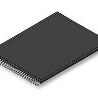
S29GL128S10TFI010 Spansion Inc., S29GL128S10TFI010 Datasheet - Page 76

S29GL128S10TFI010
Manufacturer Part Number
S29GL128S10TFI010
Description
Flash 128 MBIT 3V 100NS PAGE MODE FLASH
Manufacturer
Spansion Inc.
Datasheet
1.S29GL128S10TFI010.pdf
(97 pages)
Specifications of S29GL128S10TFI010
Data Bus Width
16 bit
Memory Type
Flash
Memory Size
128 Mbit
Architecture
Uniform
Timing Type
Asynchronous
Interface Type
CFI
Access Time
100 ns
Supply Voltage (max)
3.6 V
Supply Voltage (min)
2.7 V
Maximum Operating Current
100 mA
Operating Temperature
- 40 C to + 85 C
Mounting Style
SMD/SMT
Package / Case
TSOP-56
Lead Free Status / Rohs Status
Compliant
Available stocks
Company
Part Number
Manufacturer
Quantity
Price
Part Number:
S29GL128S10TFI010
Manufacturer:
SPANSIO
Quantity:
20 000
10.3
76
10.3.1
Power On Reset (POR) and Warm Reset
Power-On (Cold) Reset (POR)
Normal precautions must be taken for supply decoupling to stabilize the V
device in a system should have the V
the package connections (this capacitor is generally on the order of 0.1 µF).
Notes:
1. Not 100% tested.
2. Timing measured from V
3. RESET# Low is optional during POR. If RESET is asserted during POR, the later of t
4. V
5. V
6. Sum of t
During the rise of power supplies the V
voltage. However, the V
> 1.65V i.e. the V
power up, until the V
The Cold Reset Embedded Algorithm requires a relatively long, hundreds of µs, period (t
EAC algorithms and default state from non-volatile memory. During the Cold Reset period all control signals
including CE# and RESET# are ignored. If CE# is Low during t
POR current during t
of t
of t
to the Standby state.
When power is first applied, with supply voltage below V
internal device configuration and warm reset activities are initiated. CE# is ignored for the duration of the POR
operation (t
POR it must satisfy the Hardware Reset parameters t
completed at the later of t
During Cold Reset the device will draw I
Low. If RESET# remains Low after t
t
VCS
VCS
RH
CC
CC
Parameter
before CE# goes Low.
≥
and V
. RESET# may be High or Low during t
t
t
t
VIOS
to hold the device in the Hardware Reset state. If RESET# is High at the end of t
VCS
RPH
t
t
V
RP
RH
IO
RP
- 200 mV during power-up.
IO
VCS
and t
RESET#
ramp rate can be non-linear.
VCC
CE#
RH
or t
VIO
IO
must be equal to or greater than t
V
V
RESET# Low to CE# Low
RESET# Pulse Width
Time between RESET# (High) and CE# (low)
VIOS
CC
IO
supply voltage must not lag behind the V
IO
VCS
Setup Time to first access (Notes 1, 2)
Setup Time to first access (Notes 1, 2)
CC
supply voltage reaches its minimum operating level.
). RESET# Low during this POR period is optional. If RESET# is driven Low during
D a t a
IO
reaching V
but the level of CE# will not affect the Cold Reset EA. CE# must be High by the end
VCS
supply voltage must also be above V
or t
VIOS
Table 10.2 Power ON and Reset Parameters
CC
VIOS
S h e e t
, or t
GL-S MirrorBit
Description
minimum and V
CC
VCS
or t
Figure 10.3 Power-Up Diagram
IO
CC7
and V
is satisfied, t
supply voltage must remain less than or equal to the V
RPH
RPH.
current.
VCS
.
( A d v a n c e
IO
IO
®
. If RESET# is Low during t
power supplies decoupled by a suitable capacitor close to
reaching V
Family
RPH
tVCS
RP
tVIOS
is measured from the end of t
RST
and t
IO
minimum to V
then rising to reach operating range minimum,
CC
RPH
VCS
CC
supply voltage by more than 200 mV during
I n f o r m a t i o n )
S29GL_128S_01GS_00_01 February 11, 2011
. In which case the Reset operations will be
-200 mV until the V
the device may draw higher than normal
RPH
Limit
Min
Min
Min
Min
Min
IH
, t
tRH
on Reset and V
VIOS
CC
VCS
, or t
and V
VIOS
VCS
it may remain Low at the end
, or t
IO
will determine when CE# may go
VCS
IL
power supplies. Each
Value
IO
on CE#.
300
300
200
35
50
VCS
. RESET must also be High
VCS
supply voltage is
the device will go
) to load all of the
CC
supply
Unit
µs
µs
µs
ns
ns


