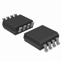
74LVC1G53DC,125 NXP Semiconductors, 74LVC1G53DC,125 Datasheet - Page 2

74LVC1G53DC,125
Manufacturer Part Number
74LVC1G53DC,125
Description
IC MUX/DEMUX 2X1 8VSSOP
Manufacturer
NXP Semiconductors
Series
74LVCr
Type
Analog Multiplexerr
Datasheet
1.74LVC1G53DC125.pdf
(27 pages)
Specifications of 74LVC1G53DC,125
Package / Case
8-VFSOP (0.091", 2.3mm Width)
Function
Multiplexer/Demultiplexer
Circuit
1 x 2:1
On-state Resistance
6 Ohm
Voltage Supply Source
Single Supply
Voltage - Supply, Single/dual (±)
1.65 V ~ 5.5 V
Current - Supply
0.1µA
Operating Temperature
-40°C ~ 125°C
Mounting Type
Surface Mount
Number Of Channels
1 Channel
On Resistance (max)
34 Ohm (Typ) @ 1.95 V
On Time (max)
6.7 ns (Typ) @ 1.95 V
Off Time (max)
6.8 ns (Typ) @ 1.95 V
Supply Voltage (max)
5.5 V
Supply Voltage (min)
1.65 V
Maximum Power Dissipation
250 mW
Maximum Operating Temperature
+ 125 C
Minimum Operating Temperature
- 40 C
Mounting Style
SMD/SMT
Number Of Switches
Single
Switch Current (typ)
0.0001 mA @ 5.5 V
Package
8VSSOP
Maximum On Resistance
195@1.95V Ohm
Maximum Propagation Delay Bus To Bus
2.5@1.95V@-40C to 125C|1.5@2.7V@-40C to 125C|1@3.6V@-40C to 125C|0.8@5.5V@-40C to 125C ns
Maximum Low Level Output Current
50 mA
Multiplexer Architecture
2:1
Maximum Turn-off Time
6.8(Typ)@1.95V ns
Maximum Turn-on Time
6.7(Typ)@1.95V ns
Power Supply Type
Single
Lead Free Status / RoHS Status
Lead free / RoHS Compliant
Lead Free Status / RoHS Status
Lead free / RoHS Compliant, Lead free / RoHS Compliant
Other names
568-3009-2
935279945125
935279945125
NXP Semiconductors
3. Ordering information
Table 1.
4. Marking
Table 2.
[1]
5. Functional diagram
74LVC1G53
Product data sheet
Type number
74LVC1G53DP −40 °C to +125 °C
74LVC1G53DC −40 °C to +125 °C
74LVC1G53GT −40 °C to +125 °C
74LVC1G53GF −40 °C to +125 °C
74LVC1G53GD −40 °C to +125 °C
74LVC1G53GM −40 °C to +125 °C
74LVC1G53GN −40 °C to +125 °C
74LVC1G53GS −40 °C to +125 °C
Type number
74LVC1G53DC
74LVC1G53DP
74LVC1G53GT
74LVC1G53GF
74LVC1G53GD
74LVC1G53GM
74LVC1G53GN
74LVC1G53GS
Fig 1.
The pin 1 indicator is located on the lower left corner of the device, below the marking code.
Logic symbol
Ordering information
Marking codes
Package
Temperature range Name
TSSOP8
VSSOP8 plastic very thin shrink small outline package; 8 leads;
XSON8
XSON8
XSON8U plastic extremely thin small outline package; no leads;
XQFN8U plastic extremely thin quad flat package; no leads;
XSON8
XSON8
All information provided in this document is subject to legal disclaimers.
Rev. 06 — 21 June 2010
Description
plastic thin shrink small outline package; 8 leads;
body width 3 mm; lead length 0.5 mm
body width 2.3 mm
plastic extremely thin small outline package; no leads;
8 terminals; body 1 × 1.95 × 0.5 mm
extremely thin small outline package; no leads;
8 terminals; body 1.35 × 1 × 0.5 mm
8 terminals; UTLP based; body 3 × 2 × 0.5 mm
8 terminals; UTLP based; body 1.6 × 1.6 × 0.5 mm
extremely thin small outline package; no leads;
8 terminals; body 1.2 × 1.0 × 0.35 mm
extremely thin small outline package; no leads;
8 terminals; body 1.35 × 1.0 × 0.35 mm
Y1
Y0
E
Marking code
V53
V53
V53
V3
V53
V53
V3
V3
001aah795
S
Z
2-channel analog multiplexer/demultiplexer
[1]
74LVC1G53
© NXP B.V. 2010. All rights reserved.
Version
SOT505-2
SOT765-1
SOT833-1
SOT1089
SOT996-2
SOT902-1
SOT1116
SOT1203
2 of 27


