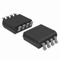
74LVC1G53DC,125 NXP Semiconductors, 74LVC1G53DC,125 Datasheet - Page 13

74LVC1G53DC,125
Manufacturer Part Number
74LVC1G53DC,125
Description
IC MUX/DEMUX 2X1 8VSSOP
Manufacturer
NXP Semiconductors
Series
74LVCr
Type
Analog Multiplexerr
Datasheet
1.74LVC1G53DC125.pdf
(27 pages)
Specifications of 74LVC1G53DC,125
Package / Case
8-VFSOP (0.091", 2.3mm Width)
Function
Multiplexer/Demultiplexer
Circuit
1 x 2:1
On-state Resistance
6 Ohm
Voltage Supply Source
Single Supply
Voltage - Supply, Single/dual (±)
1.65 V ~ 5.5 V
Current - Supply
0.1µA
Operating Temperature
-40°C ~ 125°C
Mounting Type
Surface Mount
Number Of Channels
1 Channel
On Resistance (max)
34 Ohm (Typ) @ 1.95 V
On Time (max)
6.7 ns (Typ) @ 1.95 V
Off Time (max)
6.8 ns (Typ) @ 1.95 V
Supply Voltage (max)
5.5 V
Supply Voltage (min)
1.65 V
Maximum Power Dissipation
250 mW
Maximum Operating Temperature
+ 125 C
Minimum Operating Temperature
- 40 C
Mounting Style
SMD/SMT
Number Of Switches
Single
Switch Current (typ)
0.0001 mA @ 5.5 V
Package
8VSSOP
Maximum On Resistance
195@1.95V Ohm
Maximum Propagation Delay Bus To Bus
2.5@1.95V@-40C to 125C|1.5@2.7V@-40C to 125C|1@3.6V@-40C to 125C|0.8@5.5V@-40C to 125C ns
Maximum Low Level Output Current
50 mA
Multiplexer Architecture
2:1
Maximum Turn-off Time
6.8(Typ)@1.95V ns
Maximum Turn-on Time
6.7(Typ)@1.95V ns
Power Supply Type
Single
Lead Free Status / RoHS Status
Lead free / RoHS Compliant
Lead Free Status / RoHS Status
Lead free / RoHS Compliant, Lead free / RoHS Compliant
Other names
568-3009-2
935279945125
935279945125
NXP Semiconductors
Table 11.
Table 12.
At recommended operating conditions; voltages are referenced to GND (ground = 0 V); T
74LVC1G53
Product data sheet
Supply voltage
V
1.65 V to 1.95 V
2.3 V to 2.7 V
2.7 V
3 V to 3.6 V
4.5 V to 5.5 V
Symbol
THD
f
(−3dB)
Fig 18. Load circuit for switching times
CC
Test data is given in
Definitions test circuit:
R
C
R
V
Parameter
total harmonic distortion
−3 dB frequency response R
EXT
T
L
L
Test data
Additional dynamic characteristics
= Load capacitance (including jig and probe capacitance).
= Load resistance.
= Termination resistance (should be equal to output impedance Z
= External voltage for measuring switching times.
11.2 Additional dynamic characteristics
Input
V
V
V
V
V
V
I
CC
CC
CC
CC
CC
Table
11.
t
≤ 2.0 ns
≤ 2.0 ns
≤ 2.5 ns
≤ 2.5 ns
≤ 2.5 ns
r
, t
Conditions
f
C
f
i
= 600 Hz to 20 kHz; R
L
L
V
V
V
V
V
V
V
V
All information provided in this document is subject to legal disclaimers.
G
= 50 pF; V
= 50 Ω; C
CC
CC
CC
CC
CC
CC
CC
CC
= 1.65 V
= 2.3 V
= 3.0 V
= 4.5 V
= 1.65 V
= 2.3 V
= 3.0 V
= 4.5 V
V
I
Load
C
30 pF
30 pF
50 pF
50 pF
50 pF
Rev. 06 — 21 June 2010
L
L
I
= 5 pF; see
R T
= 0.5 V (p-p); see
DUT
V
CC
L
R
1 kΩ
500 Ω
500 Ω
500 Ω
500 Ω
= 600 Ω;
V
Figure 20
L
O
o
of the pulse generator).
2-channel analog multiplexer/demultiplexer
Figure 19
C L
V
mna616
EXT
V
t
open
open
open
open
open
PLH
R L
R L
EXT
, t
PHL
amb
Min
-
-
-
-
-
-
-
-
= 25
t
GND
GND
GND
GND
GND
PZH
74LVC1G53
Typ
0.260
0.078
0.078
0.078
200
300
300
300
, t
°
C.
PHZ
© NXP B.V. 2010. All rights reserved.
Max
-
-
-
-
-
-
-
-
t
2V
2V
2V
2V
2V
PZL
CC
CC
CC
CC
CC
, t
PLZ
Unit
%
%
%
%
MHz
MHz
MHz
MHz
13 of 27


