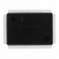
ISL54102ACQZ Intersil, ISL54102ACQZ Datasheet - Page 17

ISL54102ACQZ
Manufacturer Part Number
ISL54102ACQZ
Description
IC TMDS REGEN W/MUX 128-MQFP
Manufacturer
Intersil
Datasheet
1.ISL54101ACQZ.pdf
(21 pages)
Specifications of ISL54102ACQZ
Applications
Multimedia Displays, Test Equipment
Interface
I²C
Voltage - Supply
3 V ~ 3.6 V
Package / Case
128-MQFP, 128-PQFP
Mounting Type
Surface Mount
Rohs Compliant
Yes
Lead Free Status / RoHS Status
Lead free / RoHS Compliant
Available stocks
Company
Part Number
Manufacturer
Quantity
Price
Company:
Part Number:
ISL54102ACQZ
Manufacturer:
INTERSIL
Quantity:
2 370
Part Number:
ISL54102ACQZ
Manufacturer:
INTERSIL
Quantity:
20 000
• Minimize capacitance on all TMDS lines. The lower the
• Maintain a constant, solid ground (or power) plane under
• Ideally each supply should be bypassed to ground with a
capacitance, the sharper the rise and fall times.
the 3 high speed TMDS signals. Do not route the signals
over gaps in the ground plane or over other traces.
0.1µF capacitor. Minimize trace length and vias to
minimize inductance and maximize noise rejection.
Figure 12 demonstrates a common but non-ideal PCB
layout and its equivalent circuit. The additional trace
resistance between the bypass capacitor and the power
supply/IC reduces its effectiveness. Figure 13
demonstrates a better layout. In this case there is still
series trace resistance (it is impossible to completely
eliminate it), but now it is being put to good use, as part of
a “T” filter, attenuating supply noise before it gets to the IC,
and reducing the amount of IC-generated noise that gets
FIGURE 12. SUB-OPTIMAL BYPASS CAPACITOR LAYOUT
V
+
EQUIVALENT CIRCUIT
C
BYPASS
VIAS
GND
GROUND PLANE
TO
POWER PLANE
C
R
BYPASS
TRACE
17
POWER
PLANE
VIA TO
R
R
VIA
TRACE
GND
V
+
GND
IC
V
ISL54100A, ISL54101A, ISL54102A
+
IC
ISL5410xA Serial Communication
Overview
The ISL5410xA uses a 2-wire serial bus for communication
with its host. SCL is the Serial Clock line, driven by the host
and SDA is the Serial Data line, which can be driven by all
devices on the bus. SDA is open drain to allow multiple
devices to share the same bus simultaneously.
Communication is accomplished in three steps:
1. The Host selects the ISL5410xA it wishes to
2. The Host writes the initial ISL5410xA Configuration
3. The Host writes to or reads from the ISL5410xA’s
injected into the supply. Follow the good supply bypassing
rules shown in Figure 13 to the extent possible.
FIGURE 13. OPTIMAL (“T”) BYPASS CAPACITOR LAYOUT
communicate with.
Register address it wishes to write to or read from.
Configuration Register. The ISL5410xA’s internal
address pointer auto increments, so to read registers
0x00 through 0x1B, for example, one would write 0x00 in
step 2, then repeat step three 28 times, with each read
returning the next register value.
V
+
EQUIVALENT CIRCUIT
R
POWER
VIA TO
PLANE
VIA
C
R
BYPASS
TRACE
POWER PLANE
GROUND PLANE
C
VIAS
GND
TO
BYPASS
R
TRACE
GND
V
+
GND
IC
V
+
IC
June 17, 2008
FN6725.0


