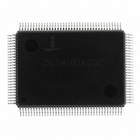
ISL54102ACQZ Intersil, ISL54102ACQZ Datasheet - Page 16

ISL54102ACQZ
Manufacturer Part Number
ISL54102ACQZ
Description
IC TMDS REGEN W/MUX 128-MQFP
Manufacturer
Intersil
Datasheet
1.ISL54101ACQZ.pdf
(21 pages)
Specifications of ISL54102ACQZ
Applications
Multimedia Displays, Test Equipment
Interface
I²C
Voltage - Supply
3 V ~ 3.6 V
Package / Case
128-MQFP, 128-PQFP
Mounting Type
Surface Mount
Rohs Compliant
Yes
Lead Free Status / RoHS Status
Lead free / RoHS Compliant
Available stocks
Company
Part Number
Manufacturer
Quantity
Price
Company:
Part Number:
ISL54102ACQZ
Manufacturer:
INTERSIL
Quantity:
2 370
Part Number:
ISL54102ACQZ
Manufacturer:
INTERSIL
Quantity:
20 000
Tx Loading Considerations
When the ISL5410xA is powered-up and its Tx outputs are
disabled, via either the PD (power-down) pin, the
power-down register bit (register 0x02[5]), or the tri-state
outputs bits (register 0x05[1:0]), the Tx pins are high
impedance. In this state they will draw no current from the
Rx pins of any TMDS receiver they may be connected to.
However if power to the ISL5410xA is removed, the Tx pins
are no longer high-impedance. Figure 10 shows the relevant
equivalent circuit, including the internal ESD protection
diodes. For simplicity, only one of the eight Tx outputs, ESD
protection diodes, and Rx termination resistors are shown.
When V
applied to the external TMDS receiver, ESD protection
diodes inside the ISL5410xA can become forward-biased,
drawing current from the external TMDS receiver it is
attached to.
3.3V
FIGURE 9. ISL54100 EYE DIAGRAM AFTER 15m CABLE
FIGURE 10. ISL5410xA ESD PROTECTION DIODES
TX
D
to the ISL5410xA drops below ~2.7V and power is
V
D
_ESD
V
D
ISL5410xA
(74, 95)
Tx
16
ISL54100A, ISL54101A, ISL54102A
Tx
N
Rx
N
3.3V
50
RX
This is non-ideal and will cause the ISL5410xA to fail HDMI
Compliance Test 7-3 (“V
each 50Ω Rx
device containing the ISL5410xA.
To prevent this leakage current, insert a Schottky diode
between the V
in Figure 11. With the addition of this diode the system will
pass compliance test 7-3.
PCB Layout Recommendations
Because of the high speed of the TMDS signals, careful
PCB layout is critical to maximize performance. The
following guidelines should be adhered to as closely as
possible:
• All TMDS pair traces should have a characteristic
• Avoid vias for all 3 high speed TMDS pairs. Vias add
• For each TMDS channel, the trace lengths of the 3 TMDS
• The trace length of the clock pair is not critical at all.
impedance of 50Ω with respect to the power/ground
planes and 100Ω with respect to each other. Failure to
meet this requirement will increase reflections, shrinking
the available eye.
inductance which causes a discontinuity in the
characteristic impedance of the trace. Keep all the traces
on the top (or the bottom) of the PCB. The TMDS clock
can have vias if necessary, since it is lower speed and less
critical. If you must use a via, ensure the vias are
symmetrical (put identical vias in both lines of the
differential pair).
pairs (0, 1 and 2) should ideally be the same to reduce
inter channel skew introduced by the board.
Since the clock is only used as a frequency reference, its
phase/delay is inconsequential. In addition, since the
TMDS clock frequency is 1/10th the pixel rate, the clock
signal itself is much more noise-immune. So liberties
(such as vias and circuitous paths) can be taken when
routing the clock lines.
3.3V
FIGURE 11. SCHOTTKY DIODE MODIFICATION
0.1μF
TX
V
D
C
D
1
_ESD
N
1
D
resistor when the power is removed from the
V
power net and the V
D
ISL5410xA
(74, 95)
OFF
”). V
Tx
OFF
D
is the voltage across
_ESD pins as shown
Tx
N
Rx
N
3.3V
June 17, 2008
50
FN6725.0
RX


