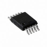
PCA9527DP,118 NXP Semiconductors, PCA9527DP,118 Datasheet - Page 5

PCA9527DP,118
Manufacturer Part Number
PCA9527DP,118
Description
IC BUFFER SHIFT DDC 3CH 10-TSSOP
Manufacturer
NXP Semiconductors
Type
Bufferr
Specifications of PCA9527DP,118
Tx/rx Type
I²C Logic
Delay Time
115ns
Capacitance - Input
8pF
Voltage - Supply
2.7 V ~ 5.5 V
Current - Supply
100mA
Mounting Type
Surface Mount
Package / Case
10-TSSOP
Operating Temperature (min)
-40C
Operating Temperature Classification
Industrial
Operating Temperature (max)
85C
Package Type
TSSOP
Rad Hardened
No
Logic Family
PCA
Number Of Channels Per Chip
3
Supply Voltage (max)
5.5 V
Supply Voltage (min)
2.7 V
Maximum Operating Temperature
+ 85 C
Mounting Style
SMD/SMT
Interface
DDC, I2C, SMBus
Minimum Operating Temperature
- 40 C
Propagation Delay Time
115 ns
Lead Free Status / RoHS Status
Lead free / RoHS Compliant
Other names
568-4770-2
Available stocks
Company
Part Number
Manufacturer
Quantity
Price
Company:
Part Number:
PCA9527DP,118
Manufacturer:
MAX
Quantity:
44
By replacing complex parallel interfaces with a straightforward yet powerful serial
structure, the I
Invented by NXP (Philips) more than 30 years ago, the I
format to carry data one bit at a time. It performs inter-chip addressing, selection,
control, and data transfer. Speeds are up to 400 kHz (Fast-mode), 1 MHz (Fast-mode
Plus), 3.4 MHz (High Speed-mode), or 5 MHz (Ultra Fast-mode).
The I
copper traces are needed, it enables a smaller PCB, reduces design complexity, and
lowers system cost.
I
address pins set high (1) or low (0). Information is transmitted byte by byte, and each byte is acknowledged by the receiver.
There can be multiple devices on the same bus, and more than one IC can act as master. The master role is typically played by a
microcontroller.
Our I
is a valuable resource for device
information and training programs.
It gives you direct access to a comprehensive
handbook, application notes, information
about evaluation kits and training
materials, links to application and
design support, and more.
The I
and daughter cards make it easy to
program new peripherals and are a quick
way to learn about the I
Write data
Read data
S = Start condition
A = Acknowledge
2
C-bus devices are available in a wide range of functions. Each slave device has its own I
S
S
2
2
2
C-bus website (www.nxp.com/interface)
C Fm+ development board
C-bus shrinks the IC footprint and leads to lower IC costs. Plus, since far fewer
slave address
slave address
2
C-bus revolutionized chip-to-chip communications.
R/W = read/write
A = Not acknowledge
W
R
2
C-bus protocol.
A
A
<
< n data >
data
data
bytes
I
2
P = Stop condition
C-bus: The serial revolution
n data bytes
A
A
data
data
last data byte
OM6275 I2C 2005-1 evaluation board with OM6293
MCU
PCA9600 Fm+ 1-MHz bus buffer daughter card
A
A
OM6281 PCA9698 Fm+ 40-bit GPIO daughter
>
PCF8576D, PCF2119, PCF8531, PCA9633
P
P
2
OM6290 LCD driver evaluation board :
C-bus uses a simple two-wire
card with PCA9530 2-bit LED dimmer
I/O
Master
transmitter
receiver
A/D
D/A
The master always sends the clock
LCD
New function address
1010A
2
SDA
SCL
SDA
SCL
C-bus address, selectable using
2
A
Parallel Interface
1
A
0
RTC
R/W
Slave
A
A
A
0
1
2
transmitter
function
receiver
New
I
2
uC
New function address
C Serial Interface
1010011 R/W
as assigned
MCU
SDA
SCL


