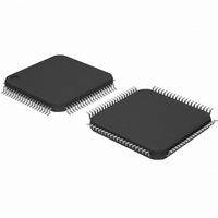
DS92LV18TVV/NOPB National Semiconductor, DS92LV18TVV/NOPB Datasheet - Page 5

DS92LV18TVV/NOPB
Manufacturer Part Number
DS92LV18TVV/NOPB
Description
IC SER/DES LVDS 18BIT BUS 80LQFP
Manufacturer
National Semiconductor
Datasheet
1.DS92LV18TVVNOPB.pdf
(20 pages)
Specifications of DS92LV18TVV/NOPB
Function
Serializer/Deserializer
Data Rate
2.38Gbps
Input Type
LVTTL/LVCMOS
Output Type
LVTTL, LVCMOS
Number Of Inputs
18
Number Of Outputs
1
Voltage - Supply
3.15 V ~ 3.45 V
Operating Temperature
-40°C ~ 85°C
Mounting Type
Surface Mount
Package / Case
80-LQFP
No. Of Inputs
18
No. Of Outputs
18
Supply Voltage Range
3.15V To 3.45V
Driver Case Style
LQFP
No. Of Pins
80
Msl
MSL 3 - 168 Hours
Termination Type
SMD
Rohs Compliant
Yes
Filter Terminals
SMD
Digital Ic Case Style
LQFP
For Use With
LVDS-18B-EVK - BOARD EVALUATION DS92LV18
Lead Free Status / RoHS Status
Lead free / RoHS Compliant
Other names
*DS92LV18TVV
*DS92LV18TVV/NOPB
DS92LV18TVV
*DS92LV18TVV/NOPB
DS92LV18TVV
Available stocks
Company
Part Number
Manufacturer
Quantity
Price
Company:
Part Number:
DS92LV18TVV/NOPB
Manufacturer:
TI
Quantity:
1 000
Company:
Part Number:
DS92LV18TVV/NOPB
Manufacturer:
TI
Quantity:
2 170
Company:
Part Number:
DS92LV18TVV/NOPB
Manufacturer:
Texas Instruments
Quantity:
10 000
Part Number:
DS92LV18TVV/NOPB
Manufacturer:
NS/国半
Quantity:
20 000
Symbol
t
t
RNMI-R
t
t
RNMI-L
Deserializer Switching Characteristics
t
t
DSR1
DSR2
t
t
Over recommended operating supply and temperature ranges unless otherwise specified.
Note 1: “Absolute Maximum Ratings” are those values beyond which the safety of the device cannot be guaranteed. They are not meant to imply that the devices
should be operated at these limits. The table of “Electrical Characteristics” specifies conditions of device operation.
Note 2: Typical values are given for V
Note 3: Current into device pins is defined as positive. Current out of device pins is defined as negative. Voltages are referenced to ground except VOD, ∆VOD,
VTH and VTL which are differential voltages.
Note 4: Due to TRI-STATE of the Serializer, the Deserializer will lose PLL lock and have to resynchronize before data transfer.
Note 5: t
present at the LVDS inputs (RI+ and RI-) before exiting powerdown mode. t
the LVDS input (RI+ and RI-) conditions change from not receiving data to receiving synchronization patterns. Both t
running and stable.
Note 6: t
in reference with the ideal bit position, please see National’s AN-1217 for detail.
Note 7: A sync pattern is a fixed pattern with 9-bits of data high followed by 9-bits of data low. The SYNC pattern is automatically generated by the transmitter when
the SYNC pin is pulled high.
Note 8: Guaranteed by Design (GBD) using statistical analysis.
Note 9: Total Interconnect Jitter Budget (t
t
Note 10: The VOD specification is a measurement of the difference between the single-ended VOH and VOL output voltages across a100 ohm load. Applying the
formula OUT+ - OUT- to the differential outputs will result in a waveform with peak to peak amplitude equal to twice the datasheet indicated VOD.
t
HZR
ZHR
LZR
ZLR
JI
DD
t
JI
is GBD using statistical analysis.
HIGH to TRI-STATE
TRI-STATE to HIGH
DSR1
RNMI
LOW to TRI-STATE
TRI-STATE to LOW
Noise Margin Right
Deserializer Delay
Total Interconnect
Noise Margin Left
Ideal Deserializer
Ideal Deserializer
Powerdown (with
Deserializer PLL
Deserializer PLL
Lock Time from
Lock time from
Jitter Budget
is a measure of how much phase noise (jitter) the deserializer can tolerate in the incoming data stream before bit errors occur. It is a measurement
is the time required by the deserializer to obtain lock when exiting powerdown mode. t
SYNCPAT)
Parameter
SYNCPAT
Delay
Delay
Delay
Delay
CC
(Note 7) (Note 8)
(Note 7) (Note 8)
(Note 6) (Note 8)
(Note 6) (Note 8)
JI
= 3.3V and T
Conditions
) specifies the allowable jitter added by the interconnect assuming both transmitter and receiver are DS92LV18 circuits.
Figure 14,
Figure 15,
Figure 13
Figure 17
Figure 17
(Note 9)
A
= +25˚C.
ROUT(0-17),
Pin/Freq.
66 MHz
66 MHz
15 MHz
66 MHz
15 MHz
66 MHz
15 MHz
66 MHz
15MHz
15MHz
LOCK
RCLK
DSR2
is the time required to obtain lock for the powered-up and enabled deserializer when
5
(Continued)
1.75*t
Min
RCP
+ 2.1
DSR1
is specified with synchronization patterns (SYNCPATs)
1.75*t
DSR1
Typ
RCP
2.2
2.2
2.3
2.9
3.7
1.9
1.5
0.9
and t
+ 4.0
DSR2
are specified with the REFCLK
1.75*t
1490
1460
1060
Max
RCP
180
330
160
10
10
10
10
10
4
5
2
+ 6.1
www.national.com
Units
ns
ns
ns
ns
ns
µs
µs
µs
µs
ps
ps
ps
ps
ps
ps


