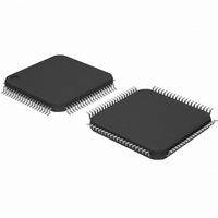
DS92LV18TVV/NOPB National Semiconductor, DS92LV18TVV/NOPB Datasheet - Page 4

DS92LV18TVV/NOPB
Manufacturer Part Number
DS92LV18TVV/NOPB
Description
IC SER/DES LVDS 18BIT BUS 80LQFP
Manufacturer
National Semiconductor
Datasheet
1.DS92LV18TVVNOPB.pdf
(20 pages)
Specifications of DS92LV18TVV/NOPB
Function
Serializer/Deserializer
Data Rate
2.38Gbps
Input Type
LVTTL/LVCMOS
Output Type
LVTTL, LVCMOS
Number Of Inputs
18
Number Of Outputs
1
Voltage - Supply
3.15 V ~ 3.45 V
Operating Temperature
-40°C ~ 85°C
Mounting Type
Surface Mount
Package / Case
80-LQFP
No. Of Inputs
18
No. Of Outputs
18
Supply Voltage Range
3.15V To 3.45V
Driver Case Style
LQFP
No. Of Pins
80
Msl
MSL 3 - 168 Hours
Termination Type
SMD
Rohs Compliant
Yes
Filter Terminals
SMD
Digital Ic Case Style
LQFP
For Use With
LVDS-18B-EVK - BOARD EVALUATION DS92LV18
Lead Free Status / RoHS Status
Lead free / RoHS Compliant
Other names
*DS92LV18TVV
*DS92LV18TVV/NOPB
DS92LV18TVV
*DS92LV18TVV/NOPB
DS92LV18TVV
Available stocks
Company
Part Number
Manufacturer
Quantity
Price
Company:
Part Number:
DS92LV18TVV/NOPB
Manufacturer:
TI
Quantity:
1 000
Company:
Part Number:
DS92LV18TVV/NOPB
Manufacturer:
TI
Quantity:
2 170
Company:
Part Number:
DS92LV18TVV/NOPB
Manufacturer:
Texas Instruments
Quantity:
10 000
Part Number:
DS92LV18TVV/NOPB
Manufacturer:
NS/国半
Quantity:
20 000
www.national.com
Symbol
Symbol
Symbol
t
t
t
t
Serializer Switching Characteristics
t
t
Over recommended operating supply and temperature ranges unless otherwise specified.
Deserializer Timing Requirements for REFCLK
Over recommended operating supply and temperature ranges unless otherwise specified.
t
Deserializer Switching Characteristics
Over recommended operating supply and temperature ranges unless otherwise specified.
RCP
RDC
ROS
ROH
CLH
CHL
t
t
RFCP
t
t
t
t
t
t
RFCP
RFDC
t
t
t
t
RFTT
SPW
HZD
ZHD
PLD
t
RJIT
DJIT
TCP
LZD
ZLD
SD
/
Receiver out Clock
ROUT (0-9) Setup
RCLK Duty Cycle
ROUT (0-9) Hold
Transition Time
Transition Time
Data to RCLK
Data to RCLK
Serializer PLL Lock Time
REFCLK Transition Time
Low-to-High
High-to-Low
CMOS/TTL
CMOS/TTL
Parameter
DO
DO
REFCLK Duty Cycle
Ratio of REFCLK to
Figure 16, (Note 8)
SYNC Pulse Width
Deterministic Jitter
TRI-STATE Delay
TRI-STATE Delay
Period
REFCLK Period
Serializer Delay
DO
DO
Random Jitter
±
±
HIGH Delay
LOW Delay
Parameter
Parameter
TRI-STATE to
TRI-STATE to
±
±
TCLK
HIGH to
LOW to
Conditions
t
CL = 15 pF
RCP
Figure 12
Figure 4
Figure 10 , R
= t
Room Temp., 3.3V,
C
Figure 7 (Note 4)
TCP
L
=10pF to GND
Conditions
Conditions
R
R
R
Figure 9,
Figure 8,
L
66 MHz
15 MHz
66 MHz
L
L
= 100Ω,
= 100Ω
= 100Ω
L
ROUT(0-17),
= 100Ω
Pin/Freq.
LOCK,
RCLK
RCLK
RCLK
(Continued)
4
t
510*t
TCP
5*t
-430
15.2
0.95
Min
Min
-40
40
−0.35*t
0.35*t
TCP
+ 1.0
TCP
15.2
Min
45
RCP
RCP
t
TCP
Typ
Typ
2.3
1.9
1.0
1.0
4.5
−0.5*t
50
0.5*t
T
+ 2.0
Typ
2.2
2.2
50
RCP
RCP
1024*t
t
TCP
6*t
Max
Max
66.7
1.05
190
10
10
10
10
70
60
6
TCP
+ 4.0
Max
66.7
55
TCP
4
4
(RMS)
Units
Units
Units
ns
ns
ns
ns
ns
ns
ns
ps
ps
ps
ns
ns
%
ns
ns
ns
ns
ns
%


