DS92LV18TVV/NOPB National Semiconductor, DS92LV18TVV/NOPB Datasheet - Page 3
DS92LV18TVV/NOPB
Manufacturer Part Number
DS92LV18TVV/NOPB
Description
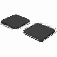
IC SER/DES LVDS 18BIT BUS 80LQFP
Manufacturer
National Semiconductor
Datasheet
1.DS92LV18TVVNOPB.pdf
(20 pages)
Specifications of DS92LV18TVV/NOPB
Function
Serializer/Deserializer
Data Rate
2.38Gbps
Input Type
LVTTL/LVCMOS
Output Type
LVTTL, LVCMOS
Number Of Inputs
18
Number Of Outputs
1
Voltage - Supply
3.15 V ~ 3.45 V
Operating Temperature
-40°C ~ 85°C
Mounting Type
Surface Mount
Package / Case
80-LQFP
No. Of Inputs
18
No. Of Outputs
18
Supply Voltage Range
3.15V To 3.45V
Driver Case Style
LQFP
No. Of Pins
80
Msl
MSL 3 - 168 Hours
Termination Type
SMD
Rohs Compliant
Yes
Filter Terminals
SMD
Digital Ic Case Style
LQFP
For Use With
LVDS-18B-EVK - BOARD EVALUATION DS92LV18
Lead Free Status / RoHS Status
Lead free / RoHS Compliant
Other names
*DS92LV18TVV
*DS92LV18TVV/NOPB
DS92LV18TVV
*DS92LV18TVV/NOPB
DS92LV18TVV
Available stocks
Company
Part Number
Manufacturer
Quantity
Price
Company:

Part Number:
DS92LV18TVV/NOPB
Manufacturer:
TI
Quantity:
1 000
Company:
Part Number:
DS92LV18TVV/NOPB
Manufacturer:
TI
Quantity:
2 170
Company:
Part Number:
DS92LV18TVV/NOPB
Manufacturer:
Texas Instruments
Quantity:
10 000
Part Number:
DS92LV18TVV/NOPB
Manufacturer:
NS/国半
Quantity:
20 000


SER/DES SUPPLY CURRENT (DVDD, PVDD and AVDD pins)
Symbol
Symbol
Symbol
Electrical Characteristics
Over recommended operating supply and temperature ranges unless otherwise specified.
Serializer Timing Requirements for TCLK
Over recommended operating supply and temperature ranges unless otherwise specified.
Serializer Switching Characteristics
Over recommended operating supply and temperature ranges unless otherwise specified.
∆V
∆V
t
t
t
t
V
V
I
I
t
t
CLKT
LLHT
LHLT
t
t
I
I
TCIH
I
CCT
CCX
TCIL
t
TCP
DIS
DIH
OS
OX
OZ
JIT
OD
OS
OD
OS
DIN (0-17) Setup to TCLK
Transmit Clock High Time
Transmit Clock Low Time
Total Supply Current (includes
Bus LVDS Low-to-High
Bus LVDS High-to-Low
Transmit Clock Period
TCLK Input Transition
Output Short Circuit Current
TRI-STATE Output Current
Supply Current Powerdown
DIN (0-17) Hold from
Output Differential Voltage
Output Differential Voltage
Offset Voltage Unbalance
Power-Off Output Current
TCLK Input Jitter
Transition Time
Transition Time
Parameter
Parameter
Offset Voltage
(DO+) - (DO-)
load current)
TCLK
Time
Parameter
Unbalance
Figure 3, (Note 8)
Figure 6, (Note 8)
C
C
L
L
=10pF to GND
=10pF to GND
Conditions
Conditions
R
R
(Continued)
VDD = 0V, DO = 0V
TPWDN and DEN =
(Note 8)
L
L
0.8V, DO = 0V OR
DO = 0V, Din = H,
TPWDN or DEN =
PWRDN = 0.8V,
= 100Ω,
= 100Ω,
REN = 0.8V
C
Conditions
R
R
R
C
Figure 18,
(Note 10),
L
L
L
L
L
or 3.6V
= 15 pF,
VDD
= 100 Ω
= 100 Ω
2.4V
= 15pF,
= 100Ω
3
f = 66 MHz, Worst
0.4T
0.4T
15.2
Min
Min
PRBS-15 pattern
2.4
(Checker-board
0
case pattern
f = 66 MHz,
DO+, DO-
Pin/Freq.
pattern)
0.5T
0.5T
Typ
Typ
0.2
0.2
T
3
1.05
Min
350
-35
-10
-10
Max
66.7
0.6T
0.6T
Max
Typ
500
190
220
±
±
0.4
0.4
1.2
2.7
-50
1.5
80
6
2
1
1
www.national.com
Max
1.25
550
320
-70
3.0
15
15
10
10
(RMS)
Units
Units
Units
ns
ns
ns
ns
ps
ns
ns
ns
ns
mV
mV
mV
mA
mA
mA
mA
µA
µA
V
Related parts for DS92LV18TVV/NOPB
Image
Part Number
Description
Manufacturer
Datasheet
Request
R

Part Number:
Description:
National Semiconductor [8-Bit D/A Converter]
Manufacturer:
National Semiconductor
Datasheet:
Part Number:
Description:
National Semiconductor [Media Coprocessor]
Manufacturer:
National Semiconductor
Datasheet:
Part Number:
Description:
Digitally Controlled Tone and Volume Circuit with Stereo Audio Power Amplifier, Microphone Preamp Stage and National 3D Sound
Manufacturer:
National Semiconductor
Datasheet:
Part Number:
Description:
Digitally Controlled Tone and Volume Circuit with Stereo Audio Power Amplifier, Microphone Preamp Stage and National 3D Sound
Manufacturer:
National Semiconductor
Datasheet:
Part Number:
Description:
AC97 Rev 2 Codec with Sample Rate Conversion and National 3D Sound
Manufacturer:
National Semiconductor
Part Number:
Description:
Manufacturer:
National Semiconductor
Datasheet:
Part Number:
Description:
Manufacturer:
National Semiconductor
Datasheet:
Part Number:
Description:
General Purpose, Low Voltage, Low Power, Rail-to-Rail Output Operational Amplifiers
Manufacturer:
National Semiconductor
Datasheet:
Part Number:
Description:
8-bit 20 MSPS flash A/D converter.
Manufacturer:
National Semiconductor
Datasheet:
Part Number:
Description:
Low Noise Quad Operational Amplifier
Manufacturer:
National Semiconductor
Datasheet:
Part Number:
Description:
Quad Differential Line Receivers
Manufacturer:
National Semiconductor
Datasheet:
Part Number:
Description:
Quad High Speed Trapezoidal? Bus Transceiver
Manufacturer:
National Semiconductor
Datasheet:
Part Number:
Description:
Dual Line Receiver
Manufacturer:
National Semiconductor
Datasheet:
Part Number:
Description:
TTL to 10k ECL Level Translator with Latch
Manufacturer:
National Semiconductor
Datasheet: