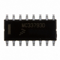
MC33793DR2 Freescale Semiconductor, MC33793DR2 Datasheet - Page 10

MC33793DR2
Manufacturer Part Number
MC33793DR2
Description
IC DSI SLAVE FOR R-SENSE 16-SOIC
Manufacturer
Freescale Semiconductor
Type
Distributed Systems Interfacer
Datasheet
1.MCZ33793EFR2.pdf
(27 pages)
Specifications of MC33793DR2
Input Type
Logic
Output Type
Logic
Interface
2 Line, I²C (CLK, Address/Data)
Mounting Type
Surface Mount
Package / Case
16-SOIC (3.9mm Width)
Lead Free Status / RoHS Status
Contains lead / RoHS non-compliant
Current - Supply
-
Lead Free Status / Rohs Status
Not Compliant
Other names
MC33793DR2TR
location that is remote from a centralized MCU. This device
provides power, measurement, and communications
between the remote sensor and the centralized MCU over a
DSI bus. Sensors such as accelerometers can be powered
from the regulated output of the device, and the resulting
analog value from the sensor can be converted from an
analog level to a digital value for transmission over the DSI
bus in response to a query from the MCU. Four I/O lines can
be configured by the central MCU over the DSI bus as analog
inputs, digital inputs, or digital outputs. This allows more than
one sensor to be remotely controlled and measured by a
single 33793. Additionally, a high drive logic output is
provided that can be used to power other low-power sensors.
board rectifiers to a storage capacitor (referred to as the
H_CAP). The H_CAP stores energy during the highest
voltage excursions of the BUSIN or BUSOUT pin (idle) and
BUS RETURN (BUSRTN)
signalling.
INPUT/OUTPUT (I/O0, I/O1, I/O2, I/O3)
input, or an analog-to-digital (A/D) input.
ANALOG GROUND (AGND)
analog-to-digital converter (ADC).
LOGIC OUT (LOGOUT)
than the standard logic I/O.
for a simplified representation of the 33793’s components.
RECTIFIER
external capacitor attached to H_CAP. The capacitor
supplies power during signaling while the input voltage is at a
lower level.
size of the filter capacitor at H_CAP must be such that the
10
33793
FUNCTIONAL DESCRIPTION
INTRODUCTION
The 33793 is designed to be used with a sensor at a
Power is passed from BUSIN or BUSOUT through on-
This pin provides the common return for power and
This pin can be used to provide a logic level output, a logic
This pin is the low reference level and power return for the
This is a logic output with higher pull-up drive capability
Refer to
This rectifier or switch peak detects the bus signal into an
The voltage waveform at BUSIN and/or BUSOUT and the
Figure
2, 33793 Internal Block Diagram, page 3,
FUNCTIONAL INTERNAL BLOCK DESCRIPTION
FUNCTIONAL DESCRIPTION
FUNCTIONAL PIN DESCRIPTION
INTRODUCTION
supplies energy to power the device during low excursions of
BUSIN and BUSOUT.
internal use, and the Power on Reset (POR) circuit provides
a reset signal during low-voltage conditions and during power
up/down. Some current is available for low-power sensors.
BUSIN and/or BUSOUT pins as voltage levels that are
sensed by the Level Detection circuitry. The Serial Decoder
detects these transitions and decodes the incoming data.
The Control Logic provides overall control of the 33793. It
controls diagnostic testing and formats responses to
commands with the message encoder. Responses are
formed via a switched current source that is slew-rate
controlled.
provides the nonvolatile storage for the pre-programmed
address. It is accessed via the Read/Write NVM command. It
has a built-in hardware lock that only allows one write.
REGULATOR OUTPUT (REGOUT)
derived from the bus.
HOLDING CAPACITOR (H_CAP)
during bus idle and supplies current to run the device and for
external devices via the REGOUT pin during non-idle
periods.
DSI BUS INPUT (BUSIN)
commands.
DSI BUS OUTPUT (BUSOUT)
initialization commands.
voltage at H_CAP will not drop below the frame threshold
during signaling.
POR
H_CAP rises above the Power-ON Reset threshold.
TIMEOUT
the input is not in idle mode. If this time exceeds a limit, the
The Regulator supplies an on-board regulated voltage for
Data from the Central Control Unit (CCU) is applied to the
The one-time programmable (OTP) memory array
This pin provides a regulated 5.0 V output. The power is
A capacitor attached to this pin is charged by the bus
This pin attaches to the bus and responds to initialization
This pin attaches to the bus and responds to reverse
The 33793 leaves the reset state when the voltage on
A timeout timer keeps track of the length of the time when
Analog Integrated Circuit Device Data
Freescale Semiconductor


