DS4550E+T&R Maxim Integrated Products, DS4550E+T&R Datasheet - Page 6
DS4550E+T&R
Manufacturer Part Number
DS4550E+T&R
Description
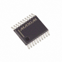
IC I/O EXPANDER I2C 9B 20TSSOP
Manufacturer
Maxim Integrated Products
Datasheet
1.DS4550ETR.pdf
(18 pages)
Specifications of DS4550E+T&R
Interface
I²C
Number Of I /o
9
Interrupt Output
No
Frequency - Clock
400kHz
Voltage - Supply
2.7 V ~ 5.5 V
Operating Temperature
-40°C ~ 85°C
Mounting Type
Surface Mount
Package / Case
20-TSSOP
Includes
EEPROM, JTAG
Lead Free Status / RoHS Status
Lead free / RoHS Compliant


I
Expander Plus Memory
6
2
PIN
10
11
12
13
14
15
16
17
18
19
20
C and JTAG Nonvolatile 9-Bit I/O
1
2
3
4
5
6
7
8
9
_____________________________________________________________________
NAME
I/O_0
I/O_1
I/O_2
I/O_3
I/O_4
I/O_5
I/O_6
I/O_7
I/O_8
GND
TCK
TMS
SDA
SCL
TDO
V
TDI
A0
A1
A2
CC
Input/Output 0. Bidirectional I/O pin.
Input/Output 1. Bidirectional I/O pin.
Input/Output 2. Bidirectional I/O pin.
Input/Output 3. Bidirectional I/O pin.
Input/Output 4. Bidirectional I/O pin.
I
I
JTAG Test Clock. This signal is used to shift data into TDI on the rising edge and out of TDO on the
falling edge.
JTAG Test Mode Select. This pin is sampled on the rising edge of TCK and used to place the TAP
into the various defined JTAG states. This pin has an internal pullup resistor.
Power Supply Voltage
I
I
JTAG Test Data Input. Test instructions and data are clocked into this pin on the rising edge of TCK.
This pin has an internal pullup resistor.
JTAG Test Data Output. Test instructions and data are clocked out of this pin on the falling edge of
TCK. If not used, this pin should be left open circuit.
I
Input/Output 5. Bidirectional I/O pin.
Input/Output 6. Bidirectional I/O pin.
Input/Output 7. Bidirectional I/O pin.
Input/Output 8. Bidirectional I/O pin.
Ground
2
2
2
2
2
C Address Input. Inputs A0, A1, and A2 determine the I
C Address Input. Inputs A0, A1, and A2 determine the I
C Address Input. Inputs A0, A1, and A2 determine the I
C Serial Data Open-Drain Input/Output
C Serial Clock Input
FUNCTION
2
2
2
C slave address of the device.
C slave address of the device.
C slave address of the device.
Pin Description
Related parts for DS4550E+T&R
Image
Part Number
Description
Manufacturer
Datasheet
Request
R

Part Number:
Description:
IC I/O EXPANDER I2C 9B 20TSSOP
Manufacturer:
Maxim Integrated Products
Datasheet:

Part Number:
Description:
Ds4550 I?c And Jtag Nonvolatile 9-bit I/o Expander Plus Memory
Manufacturer:
Maxim Integrated Products, Inc.
Datasheet:
Part Number:
Description:
power light source LUXEON® III Emitter
Manufacturer:
LUMILEDS [Lumileds Lighting Company]
Datasheet:

Part Number:
Description:
MAX7528KCWPMaxim Integrated Products [CMOS Dual 8-Bit Buffered Multiplying DACs]
Manufacturer:
Maxim Integrated Products
Datasheet:
Part Number:
Description:
Single +5V, fully integrated, 1.25Gbps laser diode driver.
Manufacturer:
Maxim Integrated Products
Datasheet:
Part Number:
Description:
Single +5V, fully integrated, 155Mbps laser diode driver.
Manufacturer:
Maxim Integrated Products
Datasheet:
Part Number:
Description:
VRD11/VRD10, K8 Rev F 2/3/4-Phase PWM Controllers with Integrated Dual MOSFET Drivers
Manufacturer:
Maxim Integrated Products
Datasheet:
Part Number:
Description:
Highly Integrated Level 2 SMBus Battery Chargers
Manufacturer:
Maxim Integrated Products
Datasheet:
Part Number:
Description:
Current Monitor and Accumulator with Integrated Sense Resistor; ; Temperature Range: -40°C to +85°C
Manufacturer:
Maxim Integrated Products
Part Number:
Description:
TSSOP 14/A°/RS-485 Transceivers with Integrated 100O/120O Termination Resis
Manufacturer:
Maxim Integrated Products
Part Number:
Description:
TSSOP 14/A°/RS-485 Transceivers with Integrated 100O/120O Termination Resis
Manufacturer:
Maxim Integrated Products
Part Number:
Description:
QFN 16/A°/AC-DC and DC-DC Peak-Current-Mode Converters with Integrated Step
Manufacturer:
Maxim Integrated Products
Part Number:
Description:
TDFN/A/65V, 1A, 600KHZ, SYNCHRONOUS STEP-DOWN REGULATOR WITH INTEGRATED SWI
Manufacturer:
Maxim Integrated Products
Part Number:
Description:
Integrated Temperature Controller f
Manufacturer:
Maxim Integrated Products
Part Number:
Description:
SOT23-6/I°/45MHz to 650MHz, Integrated IF VCOs with Differential Output
Manufacturer:
Maxim Integrated Products