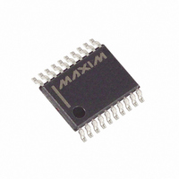
DS4550E+T&R Maxim Integrated Products, DS4550E+T&R Datasheet - Page 16

DS4550E+T&R
Manufacturer Part Number
DS4550E+T&R
Description
IC I/O EXPANDER I2C 9B 20TSSOP
Manufacturer
Maxim Integrated Products
Datasheet
1.DS4550ETR.pdf
(18 pages)
Specifications of DS4550E+T&R
Interface
I²C
Number Of I /o
9
Interrupt Output
No
Frequency - Clock
400kHz
Voltage - Supply
2.7 V ~ 5.5 V
Operating Temperature
-40°C ~ 85°C
Mounting Type
Surface Mount
Package / Case
20-TSSOP
Includes
EEPROM, JTAG
Lead Free Status / RoHS Status
Lead free / RoHS Compliant
The DS4550’s slave address of the DS4550 is deter-
mined by the state of the A0, A1, and A2 address pins
as shown in
result in a ‘0’ in the corresponding bit position in the
slave address. Conversely, address pins connected to
V
When the R/W bit is 0 (such as in A0h), the master is
indicating it will write data to the slave. If R/W = 1, (A1h
in this case), the master is indicating it wants to read
from the slave.
If an incorrect slave address is written, the DS4550
assumes the master is communicating with another I
device and ignores the communication until the next
start condition is sent.
Memory Address: During an I
master must transmit a memory address to identify the
memory location where the slave is to store the data.
The memory address is always the second byte trans-
mitted during a write operation following the slave
address byte.
Writing a Single Byte to a Slave: The master must
generate a start condition, write the slave address byte
(R/W = 0), write the memory address, write the byte of
data, and generate a stop condition. Remember the
master must read the slave’s acknowledgement during
all byte write operations.
Writing Multiple Bytes to a Slave: To write multiple
bytes to a slave, the master generates a start condition,
writes the slave address byte (R/W = 0), writes the
memory address, writes up to 8 data bytes, and gener-
ates a stop condition.
The DS4550 is capable of writing up to 8 bytes (1 page
or row) with a single I
nally controlled by an address counter that allows data
to be written to consecutive addresses without transmit-
ting a memory address before each data byte is sent.
The address counter limits the write to one 8-byte
page. Attempts to write to additional pages of memory
without sending a stop condition between pages
results in the address counter wrapping around to the
beginning of the present row. The first row begins at
address 00h and subsequent rows begin at multiples of
8 there on (08h, 10h, 18h, 20h, etc).
To prevent address wrapping from occurring, the mas-
ter must send a stop condition at the end of the page,
and then wait for the bus free or EEPROM write time to
I
Expander Plus Memory
16
CC
2
C and JTAG Nonvolatile 9-Bit I/O
result in a ‘1’ in the corresponding bit positions.
____________________________________________________________________
Figure
2. Address pins connected to GND
2
C write transaction. This is inter-
I
2
2
C Communication
C write operation, the
2
C
elapse. Then the master can generate a new start con-
dition, write the slave address byte (R/W = 0), and the
first memory address of the next memory row before
continuing to write data.
Acknowledge Polling: Any time an EEPROM page is
written, the DS4550 requires the EEPROM write time
(t
page to EEPROM. During the EEPROM write time, the
device does not acknowledge its slave address
because it is busy. It is possible to take advantage of
this phenomenon by repeatedly addressing the
DS4550, which allows communication to continue as
soon as the DS4550 is ready. The alternative to
acknowledge polling is to wait for a maximum period of
t
EEPROM Write Cycles: When EEPROM writes occur
using the I
EEPROM memory page even if only a single byte on a
page was modified. Writes that do not modify all 8
bytes on the page are valid and do not corrupt any
other bytes on the same page. Because the whole
page is written, even bytes on the page that were not
modified during the transaction are still subject to a
write cycle. The DS4550’s EEPROM write cycles are
specified in the Nonvolatile Memory Characteristics
table. The specification shown is at the worst-case tem-
perature. It is capable of handling many more writes at
room temperature.
Reading a Single Byte from a Slave: Unlike the write
operation that uses the specified memory address byte
to define where the data is to be written, the read oper-
ation occurs at the present value of the memory
address counter. To read a single byte from the slave,
the master generates a start condition, writes the slave
address byte with R/W = 1, reads the data byte with a
NACK to indicate the end of the transfer, and generates
a stop condition. However, since requiring the master
to keep track of the memory address counter is imprac-
tical, the following method should be used to perform
reads from a specified memory location.
Manipulating the Address Counter for Reads: A
dummy write cycle can be used to force the address
counter to a particular value. To do this, the master gen-
erates a start condition, writes the slave address byte
(R/W = 0), writes the memory address where it desires
to read, generates a repeated start condition, writes the
slave address byte (R/W = 1), reads data with ACK or
NACK as applicable, and generates a stop condition.
WR
WR
) after the stop condition to write the contents of the
to elapse before attempting to access the device.
2
C interface, the DS4550 writes the whole


