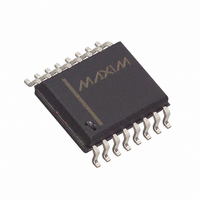
MAX7329AWE+T Maxim Integrated Products, MAX7329AWE+T Datasheet - Page 9

MAX7329AWE+T
Manufacturer Part Number
MAX7329AWE+T
Description
IC I/O EXPANDER I2C 8B 16SOIC
Manufacturer
Maxim Integrated Products
Datasheet
1.MAX7329AWE.pdf
(13 pages)
Specifications of MAX7329AWE+T
Interface
I²C
Number Of I /o
8
Interrupt Output
Yes
Frequency - Clock
100KHz
Voltage - Supply
2.5 V ~ 5.5 V
Operating Temperature
-40°C ~ 125°C
Mounting Type
Surface Mount
Package / Case
16-SOIC (0.300", 7.5mm Width)
Lead Free Status / RoHS Status
Lead free / RoHS Compliant
occur during the transmission are detected. INT always
remains high until a STOP condition.
The master can read 2 bytes from the MAX7328 or
MAX7329 and then issue the STOP condition (Figure 9).
In this case, the MAX7328 or MAX7329 transmits the cur-
rent port data repeatedly. INT goes high during the port
data-byte acknowledge. The new snapshot data is the
current port data transmitted to the master; therefore,
any port transitions that occur during the transmission
are detected. INT remains high until the STOP condition.
A data write to the MAX7328 or MAX7329 comprises the
transmission of the MAX7328’s or MAX7329’s slave
address with the R/W bit set to zero, followed by one or
more bytes of data. The MAX7328 or MAX7329 acknowl-
edges the slave address and any subsequent bytes of
data until the master issues a STOP condition (Figure 10).
The MAX7328/MAX7329’s SDA, SCL, AD0, AD1, AD2,
RST, and P0–P7 I/Os remain high impedance with up to
+6V asserted on them when the MAX7328 or MAX7329 is
powered down (V+ = 0V). The MAX7328/MAX7329 can
therefore be used in hot-swap applications.
Figure 9. Reading from the MAX7328/MAX7329 (2 Data Bytes)
t
IV
PORT INPUT DATA
INT OUTPUT
SCL
S
Writing to the MAX7328/MAX7329
ACKNOWLEDGE FROM MAX7328/MAX7329
Applications Information
MAX7328/MAX7329 SLAVE ADDRESS
_______________________________________________________________________________________
I
2
C Port Expanders with Eight I/O Ports
DATA 1
PORT SNAPSHOT DATA
R/W
1
Hot Insertion
A
t
IR
PORT SNAPSHOT
TAKEN
t
PH
P7
D7
P6
DATA 2
D6
t
IV
P5
D5
S = START CONDITION
P = STOP CONDITION
P4
DATA 1
D4
P3
D3
DATA 3
PORT SNAPSHOT
P2
D2
Each of the I/O ports P0–P7 has protection diodes to V+
and GND. When a port output is back driven to a volt-
age higher than V+ or lower than GND, the appropriate
protection diode clamps the output to a diode drop
above V+ or below GND. When a MAX7328 or MAX7329
is powered down (V+ = 0V), each output port’s protec-
tion diodes to V+ and GND continue to appear as a
diode clamp from each output to GND (Figure 1).
The MAX7328/MAX7329 operate with a 2.5V to 5.5V
power-supply voltage over the -40°C to +125°C temper-
ature range. Bypass the power supply to GND with a
ceramic capacitor of at least 0.047µF as close to the
device as possible.
PROCESS: BiCMOS
P1
D1
TAKEN
P0
D0
t
PSU
SHADED = SLAVE TRANSMISSION
N = NOT ACKNOWLEDGE
A
t
IR
ACKNOWLEDGE FROM
MASTER
P7
D7 D6
P6
Power-Supply Considerations
P5
D5
P4
D4
DATA 4
DATA 4
P3
D3
PORT SNAPSHOT
P2
D2
Chip Information
P1
D1 D0
TAKEN
P0
A
ACKNOWLEDGE FROM
MASTER
PORT
SNAPSHOT DATA
P
9


