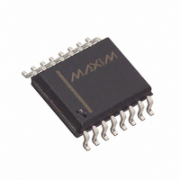
MAX7329AWE+T Maxim Integrated Products, MAX7329AWE+T Datasheet - Page 2

MAX7329AWE+T
Manufacturer Part Number
MAX7329AWE+T
Description
IC I/O EXPANDER I2C 8B 16SOIC
Manufacturer
Maxim Integrated Products
Datasheet
1.MAX7329AWE.pdf
(13 pages)
Specifications of MAX7329AWE+T
Interface
I²C
Number Of I /o
8
Interrupt Output
Yes
Frequency - Clock
100KHz
Voltage - Supply
2.5 V ~ 5.5 V
Operating Temperature
-40°C ~ 125°C
Mounting Type
Surface Mount
Package / Case
16-SOIC (0.300", 7.5mm Width)
Lead Free Status / RoHS Status
Lead free / RoHS Compliant
ABSOLUTE MAXIMUM RATINGS
(Voltage with respect to GND.)
V+, SCL, SDA, AD0, AD1, AD2, INT ........................-0.3V to +6V
P0–P7 ...........................................................-0.3V to (V+ + 0.3V)
P0–P7, SDA, INT Output Sink Current ................................25mA
SCL, SDA, AD0, AD1, AD2, INT, P0–P7 Input Current .......20mA
Total V+ Current................................................................100mA
Total GND Current ............................................................100mA
I
Stresses beyond those listed under “Absolute Maximum Ratings” may cause permanent damage to the device. These are stress ratings only, and functional
operation of the device at these or any other conditions beyond those indicated in the operational sections of the specifications is not implied. Exposure to
absolute maximum rating conditions for extended periods may affect device reliability.
ELECTRICAL CHARACTERISTICS
(Typical Operating Circuit, V+ = 2.5V to 5.5V, T
(Note 1)
2
Operating Supply Voltage
Supply Current (Interface
Running)
Standby Current (Interface Idle)
Power-On Reset Voltage
Inp ut Low V ol tag e
S D A, S C L, AD 0, AD 1, AD 2, P 0–P 7
Inp ut H i g h V ol tag e
S D A, S C L, AD 0, AD 1, AD 2, P 0–P 7
Maximum Allowed Input Current
through Protection Diode P0–P7
Output Low Current SDA
Inp ut Leakag e C ur r ent
S D A, S C L, AD 0, AD 1, AD 2, P 0–P 7
Input Capacitance
SDA, SCL, AD0, AD1, AD2
Port Output-Low Output Current
P0–P7
Ports Output-High Output Current
P0–P7
Output-High Transient Pullup
Current P0–P7
Input Capacitance P0–P7
Interrupt Output-Low Current INT
2
_______________________________________________________________________________________
C Port Expanders with Eight I/O Ports
PARAMETER
SYMBOL
I
I
I
I
PPROT
OLSDA
V
OLINT
IH
C
I
I
V
V
I
V+
OHt
C
POR
OH
I+
I+
OL
I2C
, I
IH
IL
P
IL
A
= T
f
GND
S C L, S DA, and other d i gi tal i nputs at V+ or GN D
V
Pin at V+ or GND
Pin at GND (Note 2)
V
V
Sources during acknowledge, V
V+ = 2.5V
(Note 2)
V
SCL
SDA
OL
OH
OLINT
MIN
= 1V, V+ = 5V
= 100kHz, other digital inputs at V+ or
= GND
= 0.4V
to T
= 0.4V
MAX
, unless otherwise noted. Typical values are at V+ = 5V, T
CONDITIONS
Continuous Power Dissipation (T A = +70°C)
Operating Temperature Range .........................-40°C to +125°C
Junction Temperature ......................................................+150°C
Storage Temperature Range .............................-65°C to +150°C
Lead Temperature (soldering, 10s) .................................+300°C
16-Pin Wide SO (derate 9.5mW/°C over +70°C) .........762mW
20-Pin SSOP (derate 8mW/°C over +70°C) .................640mW
20-Pin TSSOP (derate 11mW/°C over +70°C) .............879mW
OH
= GND,
0.7 x
-0.25
MIN
2.5
1.6
V+
10
30
3
TYP
1.3
40
25
1
1
+0.25
±400
MAX
0.3 x
100
300
5.5
2.4
V+
10
10
7
A
= +25°C.)
UNITS
mA
mA
mA
mA
µA
µA
µA
µA
pF
µA
pF
V
V
V
V


