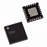
PCA9502BS,157 NXP Semiconductors, PCA9502BS,157 Datasheet - Page 3

PCA9502BS,157
Manufacturer Part Number
PCA9502BS,157
Description
IC I/O EXPANDER I2C/SPI 24HVQFN
Manufacturer
NXP Semiconductors
Datasheet
1.PCA9502BS157.pdf
(25 pages)
Specifications of PCA9502BS,157
Interface
I²C, SPI
Number Of I /o
8
Interrupt Output
No
Frequency - Clock
400kHz
Voltage - Supply
2.3 V ~ 3.6 V
Operating Temperature
-40°C ~ 85°C
Mounting Type
Surface Mount
Package / Case
24-VQFN Exposed Pad, 24-HVQFN, 24-SQFN, 24-DHVQFN
Lead Free Status / RoHS Status
Lead free / RoHS Compliant
Other names
935281363157
PCA9502BS
PCA9502BS
PCA9502BS
PCA9502BS
NXP Semiconductors
6. Pinning information
PCA9502_3
Product data sheet
6.1 Pinning
6.2 Pin description
Table 2.
Symbol
RESET
V
I2C/SPI
CS/A0
SI/A1
SO
SCL/SCLK
SDA
Fig 3. Pin configuration for HVQFN24
DD
index area
terminal 1
a. I
RESET
V
V
V
2
DD
DD
DD
A0
A1
C-bus interface
Pin description
1
2
3
4
5
6
Pin
1
2, 3, 11,
22, 24
4
5
6
7
8
9
Transparent top view
PCA9502BS
Rev. 03 — 13 October 2006
Type Description
I
-
I
I
I
O
I
I/O
device hardware reset (active LOW)
power supply
I
pin is at logic HIGH. SPI interface is selected if this pin is at logic
LOW.
SPI chip select or I
configuration is selected by I2C/SPI pin, this pin is the SPI chip
select pin (Schmitt trigger, active LOW). If I
is selected by I2C/SPI pin, this pin along with A1 pin allows user
to change the device’s base address.
SPI data input pin or I
configuration is selected by I2C/SPI pin, this is the SPI data input
pin. If I
along with A0 pin allows user to change the device’s base
address. To select the device address, please refer to
SPI data output pin. If SPI configuration is selected by I2C/SPI
pin, this is a 3-stateable output pin. If I
selected by I2C/SPI pin, this pin function is undefined and must
be left as n.c. (not connected).
I
I
selected by I2C/SPI pin. If SPI configuration is selected then this
pin is an undefined pin and must be connected to V
2
2
2
C-bus or SPI interface select. I
C-bus or SPI input clock.
C-bus data input/output, open-drain if I
18
17
16
15
14
13
002aab839
GPIO4
V
GPIO3
GPIO2
GPIO1
GPIO0
2
C-bus configuration is selected by I2C/SPI pin, this pin
SS
8-bit I/O expander with I
2
C-bus device address select A0. If SPI
index area
terminal 1
2
b. SPI interface
C-bus device address select A1. If SPI
RESET
V
V
V
CS
DD
DD
SS
SI
1
2
3
4
5
6
2
C-bus interface is selected if this
Transparent top view
[1]
PCA9502BS
2
C-bus configuration is
2
C-bus configuration is
2
2
C-bus/SPI interface
C-bus configuration
PCA9502
© NXP B.V. 2006. All rights reserved.
SS
18
17
16
15
14
13
.
Table
002aab840
GPIO4
V
GPIO3
GPIO2
GPIO1
GPIO0
SS
3 of 25
11.


