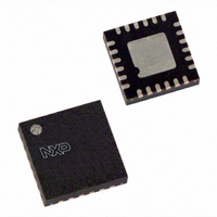
PCA9502BS,157 NXP Semiconductors, PCA9502BS,157 Datasheet - Page 11

PCA9502BS,157
Manufacturer Part Number
PCA9502BS,157
Description
IC I/O EXPANDER I2C/SPI 24HVQFN
Manufacturer
NXP Semiconductors
Datasheet
1.PCA9502BS157.pdf
(25 pages)
Specifications of PCA9502BS,157
Interface
I²C, SPI
Number Of I /o
8
Interrupt Output
No
Frequency - Clock
400kHz
Voltage - Supply
2.3 V ~ 3.6 V
Operating Temperature
-40°C ~ 85°C
Mounting Type
Surface Mount
Package / Case
24-VQFN Exposed Pad, 24-HVQFN, 24-SQFN, 24-DHVQFN
Lead Free Status / RoHS Status
Lead free / RoHS Compliant
Other names
935281363157
PCA9502BS
PCA9502BS
PCA9502BS
PCA9502BS
NXP Semiconductors
PCA9502_3
Product data sheet
9.3 Addressing
9.4 Use of sub-addresses
Before any data is transmitted or received, the master must send the address of the
receiver via the SDA line. The first byte after the START condition carries the address of
the slave device and the read/write bit.
be selected by using A1 and A0 pins. For example, if these 2 pins are connected to V
then the PCA9502’s address is set to 0x90, and the master communicates with it through
this address.
Table 11.
[1]
When a master communicates with the PCA9502 it must send a sub-address in the byte
following the slave address byte. This sub-address is the internal address of the word the
master wants to access for a single byte transfer, or the beginning of a sequence of
locations for a multi-byte transfer. A sub-address is an 8-bit byte. Unlike the device
address, it does not contain a direction (R/W) bit, and like any byte transferred on the bus
it must be followed by an acknowledge.
A register write cycle is shown in
byte with the direction bit set to ‘write’, a sub-address byte, a number of data bytes, and a
STOP signal. The sub-address indicates which register the master wants to access. and
the data bytes which follow will be written one after the other to the sub-address location.
A1
V
V
V
V
V
V
V
V
SCL
SCL
SCL
SCL
SDA
SDA
SDA
SDA
DD
DD
DD
DD
SS
SS
SS
SS
X = logic 0 for write cycle; X = logic 1 for read cycle.
PCA9502 address map
A0
V
V
SCL
SDA
V
V
SCL
SDA
V
V
SCL
SDA
V
V
SCL
SDA
DD
SS
DD
SS
DD
SS
DD
SS
Rev. 03 — 13 October 2006
PCA9502 I
0x90 (1001 000X)
0x92 (1001 001X)
0x98 (1001 100X)
0x9A (1001 101X)
0xA0 (1010 000X)
0xA2 (1010 001X)
0xA8 (1010 100X)
0xAA (1010 101X)
0x94 (1001 010X)
0x96 (1001 011X)
0x9C (1001 110X)
0x9E (1001 111X)
0xA4 (1010 010X)
0xA6 (1010 011X)
0xAC (1010 110X)
0xAE (1010 111X)
2
Figure
C-bus addresses (hex)
Table 11
10. The START is followed by a slave address
8-bit I/O expander with I
shows how the PCA9502’s address can
[1]
2
C-bus/SPI interface
PCA9502
© NXP B.V. 2006. All rights reserved.
11 of 25
DD
,


