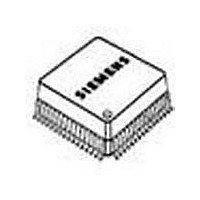
PEB24902HV2.1XT Infineon Technologies, PEB24902HV2.1XT Datasheet - Page 21

PEB24902HV2.1XT
Manufacturer Part Number
PEB24902HV2.1XT
Description
Manufacturer
Infineon Technologies
Datasheet
1.PEB24902HV2.1XT.pdf
(52 pages)
Specifications of PEB24902HV2.1XT
Number Of Line Interfaces
1
Lead Free Status / Rohs Status
Compliant
3.2
All timing signals are derived from a 15.36 MHz system clock. The 15.36 MHz clock can
be provided by the IEC-4-AFE-X Version 3.2 by a crystal based PLL, which is
synchronized to either an 8 kHz or a 2048 kHz clock at pin CLOCK. The frequency at pin
CLOCK is detected automatically.
The PLL is set to the nominal frequency either by a POR or by a falling edge at the RES
pin. When the reference clock (CLOCK) is applied, the PLL starts to synchronize.
The 15.36 MHz clock can also be provided externally at pin CL15 without making use of
the internal PLL. In this mode the pin XIN must be tied to either VDD or GND. An internal
power-on-reset circuitry assures that the pin CL15 is an input until a 15.36 MHz clock is
detected at the output of the PLL/oscillator.
To enable error-free data transport to/from the Quad IEC DFE-T/Q, the clocks DCL and
FSC from the IOM
it is recommended to use the same signal for FSC and as input to CLOCK pin at the IEC-
4-AFE-X Version 3.2 when the internal PLL is used to generate the 15.36 MHz clock.
If another clock source is used for CLOCK, e.g. the 2048 kHz DCL, a common time base
must be guaranteed. This is usually achieved if FSC is derived from DCL by dividing it
directly by 256.
Any constant phase difference between the time bases of both clocks is possible, but the
devices have currently been qualified and released only for using the same FSC signal
for the Quad IEC DFE-T/Q and for IEC-4-AFE-X Version 3.2.
3.2.1
The PLL is based on a crystal connected to the pins XIN and XOUT. For synchronization
of the 15.36 MHz clock up to 16 internal capacitances are connected to XIN and XOUT.
The loop filter of the PLL is of second order, therefore a sinusoidal input jitter with the
angular frequency
formula:
H(j ) = [(2 /
H(j ) is the complex jitter transfer factor
The maximum phase difference between the external CLOCK and the internal reference,
derived from the master clock, due to a sinusoidal input jitter with the angular frequency
difference are illustrated below:
Data Sheet
r
is the damping factor of the PLL
is given as 1 - H(j ). The magnitude of the jitter transfer function and of the phase
= 2 f
r
is the angular resonance frequency of the PLL
Clock Generation
Specification of the PLL and the 15.36 MHz Master Clock (Pin
CL15)
r
)j + 1] / [(j /
®
-2-interface must be synchronous to the 15.36 MHz signal. Therefore
= 2 f at CLOCK is attenuated by the PLL according to the following
r
2 /
r
)j + 1]
21
Functional Description
Rev. 1, 2004-05-28
PEB 24902
PEF 24902


