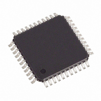
DS2148T+ Maxim Integrated Products, DS2148T+ Datasheet - Page 46

DS2148T+
Manufacturer Part Number
DS2148T+
Description
IC LIU E1/T1/J1 5V 44-TQFP
Manufacturer
Maxim Integrated Products
Type
Line Interface Units (LIUs)r
Specifications of DS2148T+
Number Of Drivers/receivers
1/1
Protocol
T1/E1/J1
Voltage - Supply
4.75 V ~ 5.25 V
Mounting Type
Surface Mount
Package / Case
44-TQFP, 44-VQFP
Lead Free Status / RoHS Status
Lead free / RoHS Compliant
DS2148/DS21Q48
7 ANALOG INTERFACE
7.1 Receiver
The DS2148 contains a digital clock recovery system. The DS2148 couples to the receive E1 or T1
twisted pair (or coaxial cable in 75Ω E1 applications) via a 1:1 transformer. See
Table 7-3
or transformer
details.
Figure
7-1,
Figure
7-2, and
Figure 7-3
along with
Table 7-1
and
Table 7-2
show the receive
termination requirements. The DS2148 has the option of using internal termination resistors.
The DS2148 is designed to be fully software-selectable for E1 and T1 without the need to change any
external resistors for the receive-side. The receive-side will allow the user to configure the DS2148 for
75Ω, 100Ω, or 120Ω receive termination by setting the RT1 (CCR5.1) and RT0 (CCR5.0) bits. When
using the internal termination feature, the Rr resistors should be 60Ω each
(Figure
7-1). If external
termination is required, RT1 and RT0 should be set to 0 and both Rr resistors in
Figure 7-1
will need to
be 37.5Ω, 50Ω, or 60Ω each depending on the line impedance.
The resultant E1 or T1 clock derived from the 2.048/1.544 PLL (JACLK in
Figure
1-1) is internally
multiplied by 16 via another internal PLL and fed to the clock recovery system. The clock recovery
system uses the clock from the PLL circuit to form a 16 times oversampler, which is used to recover the
clock and data. This oversampling technique offers outstanding performance to meet jitter tolerance
specifications shown in
Figure
7-6.
Normally, the clock that is output at the RCLK pin is the recovered clock from the E1 AMI/HDB3 or T1
AMI/B8ZS waveform presented at the RTIP and RRING inputs. When no signal is present at RTIP and
RRING, a Receive Carrier Loss (RCL) condition will occur and the RCLK will be derived from the
JACLK source
(Figure
1-1). If the jitter attenuator is placed in the receive path (as is the case in most
applications), the jitter attenuator restores the RCLK to an approximate 50% duty cycle. If the jitter
attenuator is either placed in the transmit path or is disabled, the RCLK output can exhibit slightly shorter
high cycles of the clock. This is due to the highly oversampled digital clock recovery circuitry. See the
Receive AC Timing Characteristics in Section
10
for more details.
The receive-side circuitry also contains a clock synthesizer, which outputs a user configurable clock (up
to 16.384MHz) synthesized to RCLK at BPCLK (pin 31). See
Table 4-3
for details on output clock
frequencies at BPCLK. In hardware mode, BPCLK defaults to a 16.384MHz output.
The DS2148 has a bypass mode for the receive side clock and data. This allows the BPCLK to be derived
from RCLK after the jitter attenuator while the clock and data presented at RCLK, RPOS, and RNEG go
unaltered. This is intended for applications where the receive side jitter attenuation will be done after the
LIU. Setting RJAB (CCR6.3) to a logic 1 will enable the bypass. Be sure that the jitter attenuator is in the
receive path (CCR4.3 = 0). See
Figure 1-1
for details.
The DS2148 will report the signal strength at RTIP and RRING in 2.5dB increments via RL3-RL0
located in the Receive Information Register 2. This feature is helpful when trouble shooting line
performance problems. See
Table 5-2
for details.
Monitor applications in both E1 and T1 require various flat gain settings for the receive-side circuitry.
The DS2148 can be programmed to support these applications via the Monitor Mode control bits MM1
and MM0. When the monitor modes are enabled, the receiver will tolerate normal line loss up to –6dB.
See
Table 4-4
for details.
46 of 73


