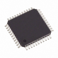
DS2148T+ Maxim Integrated Products, DS2148T+ Datasheet - Page 32

DS2148T+
Manufacturer Part Number
DS2148T+
Description
IC LIU E1/T1/J1 5V 44-TQFP
Manufacturer
Maxim Integrated Products
Type
Line Interface Units (LIUs)r
Specifications of DS2148T+
Number Of Drivers/receivers
1/1
Protocol
T1/E1/J1
Voltage - Supply
4.75 V ~ 5.25 V
Mounting Type
Surface Mount
Package / Case
44-TQFP, 44-VQFP
Lead Free Status / RoHS Status
Lead free / RoHS Compliant
CCR5 (04H): COMMON CONTROL REGISTER 5
Table 4-3. Backplane Clock Select
Table 4-4. Monitor Gain Settings
(CCR5.7)
(CCR5.5)
BPCS1
SYMBOL
(MSB)
BPCS1
RSCLKE
TSCLKE
MM1
BPCS1
BPCS0
MM1
MM0
RT1
RT0
0
0
1
1
0
0
1
1
BPCS0
(CCR5.6)
(CCR5.4)
BPCS0
POSITION
MM0
CCR5.5
CCR5.4
CCR5.7
CCR5.6
CCR5.3
CCR5.2
CCR5.1
CCR5.0
0
1
0
1
0
1
0
1
MM1
FREQUENCY
INTERNAL LINEAR GAIN
DESCRIPTION
Backplane Clock Select 1. See
Backplane Clock Select 0. See
Monitor Mode 1. See
Monitor Mode 0. See
Receive Synchronization Clock Enable. This control bit determines
whether the line receiver should handle normal T1/E1 signals or a
synchronized signal.
E1 mode:
0 = receive normal E1 signal (Section 6 of G.703)
1 = receive 2.048 MHz synchronization signal (Section 10 of G.703)
T1 mode:
0 = receive normal T1 signal
1 = receive 1.544 MHz synchronization signal
Transmit Synchronization Clock Enable. This control bit determines
whether the transmitter should transmit normal T1/E1 signals or a
synchronized signal.
E1 mode:
0 = transmit normal E1 signal (Section 6 of G.703)
1 = transmit 2.048 MHz synchronization signal (Section 10 of G.703)
T1 mode:
0 = transmit normal T1 signal
1 = transmit 1.544 MHz synchronization signal
Receive Termination 1. See
Receive Termination 0. See
16.384MHz
Normal operation (no boost)
8.192MHz
4.096MHz
2.048MHz
BPCLK
BOOST (dB)
MM0
20
26
32
32 of 73
RSCLKE
Table
Table
4-4.
4-4.
Table 4-5
Table 4-5
Table 4-3
Table 4-3
TSCLKE
for details.
for details.
for details.
for details.
RT1
(LSB)
RT0


