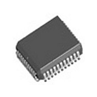
AN82527F8 Intel, AN82527F8 Datasheet - Page 13

AN82527F8
Manufacturer Part Number
AN82527F8
Description
IC CAN CONTRL 5V AUTOTEMP 44PLCC
Manufacturer
Intel
Specifications of AN82527F8
Rohs Status
RoHS non-compliant
Controller Type
Serial Communications Controller (SCC)
Interface
Serial
Voltage - Supply
4.5 V ~ 5.5 V
Current - Supply
50mA
Operating Temperature
-40°C ~ 125°C
Mounting Type
Surface Mount
Package / Case
44-PLCC
Lead Free Status / Rohs Status
Not Compliant
Other names
820732
Available stocks
Company
Part Number
Manufacturer
Quantity
Price
A C Characteristics for 8-Bit Non-Multiplexed Asynchronous (Mode 3)
Conditions V
NOTES
E and AS must be tied high in this mode
1 Definition of ‘‘Read Cycle without a Previous Write’’ The time between the rising edge of CS
cycle) and the falling edge of CS
2 Definition of ‘‘Write Cycle without a Previous Write’’ The time between the rising edge of CS
cycle) and the rising edge of CS
3 An on-chip pullup will drive DSACK0
voltage
4 Definition of CD
1 t
1 t
1 t
t
t
t
t
t
t
t
t
t
t
t
t
t
t
t
t
t
t
Symbol
AVCL
CLDV
KLDV
CHDV
CHDH
CHDZ
CHKH 1
CHKH 2
CHKZ
CHCL
CHAI
CHRI
CLCH
DVCH
CLKL
CHKL
COPD
CHCL
XTAL
SCLK
MCLK
Oscillator Frequency
System Clock Frequency
Memory Clock Frequency
Address or R W
Setup
CS
for High Speed Registers (02H 04H 05H)
For Low Speed Registers
(Read Cycle without Previous Write)
For Low Speed Registers
(Read Cycle with Previous Write)
DSACK0
for High Speed Read Register
For Low Speed Read Register
82527 Input Data Hold after CS
82527 Output Data Hold after CS
CS
CS
CS
CS
CS
CS
CS
CS
CPU Write Data Valid to CS
CS
for High Speed Registers and Low Speed
Registers Write Access without Previous
Write
End of Previous Write (CS
DSACK0
Previous Write
CLKOUT Period
CLKOUT High Period
CC
(2)
V
Low to Data Valid
High to Output Data Float
High to DSACK0
High to DSACK0
High to DSACK0
Width between Successive Cycles
High to Address Invalid
High to R W
Width Low
Low to DSACK0
e
is the value loaded in the CLKOUT register representing the CLKOUT divisor
5V
Low to Output Data Valid
Low for a Write Cycle with a
g
(2)
10% V
Parameter
Valid to CS
(for the current write cycle) is greater than 2 t
(for the current read cycle) is greater than 2 t
Invalid
SS
Low
Float
e
e
e
to approximately 2 4V An external pullup is required to drive this signal to a higher
2 4V
2 8V
High) to
0V T
High
(3)
Low
(1)
High
A
High
(1)
e b
40 C to
(CD
V
a
a
125 C C
1)
8 MHz
4 MHz
2 MHz
k
15 ns
25 ns
65 ns
20 ns
3 ns
0 ns
0 ns
0 ns
0 ns
0 ns
0 ns
7 ns
5 ns
0 ns
0 ns
Min
0 ns
t
OSC
MCLK
(CD
MCLK
L
e
b
V
100 pF
a
10 (CD
1) t
OSC (4)
1 5 t
3 5 t
V
2 t
a
MCLK
(for the previous write
(for the previous write
MCLK
MCLK
1)
16 MHz
10 MHz
150 ns
100 ns
8 MHz
55 ns
23 ns
35 ns
55 ns
67 ns
Max
a
a
a
145 ns
t
100 ns
100 ns
OSC
82527
a
15
13


