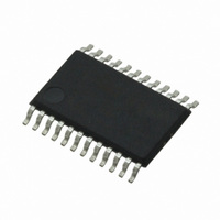
CS4270-DZZ Cirrus Logic Inc, CS4270-DZZ Datasheet - Page 28

CS4270-DZZ
Manufacturer Part Number
CS4270-DZZ
Description
IC CODEC 24BIT 105DB 24TSSOP
Manufacturer
Cirrus Logic Inc
Type
Stereo Audior
Specifications of CS4270-DZZ
Data Interface
Serial
Resolution (bits)
24 b
Number Of Adcs / Dacs
2 / 2
Sigma Delta
Yes
Dynamic Range, Adcs / Dacs (db) Typ
105 / 105
Voltage - Supply, Analog
3.1 V ~ 5.25 V
Voltage - Supply, Digital
3.1 V ~ 5.25 V
Operating Temperature
-40°C ~ 85°C
Mounting Type
Surface Mount
Package / Case
24-TSSOP
Audio Codec Type
Stereo
No. Of Adcs
1
No. Of Dacs
1
No. Of Input Channels
3
No. Of Output Channels
3
Adc / Dac Resolution
24bit
Sampling Rate
216kSPS
Ic Interface Type
I2C
Lead Free Status / RoHS Status
Lead free / RoHS Compliant
For Use With
598-1002 - BOARD EVAL FOR CS4270 CODEC
Lead Free Status / RoHS Status
Lead free / RoHS Compliant, Lead free / RoHS Compliant
Other names
598-1622
Available stocks
Company
Part Number
Manufacturer
Quantity
Price
Company:
Part Number:
CS4270-DZZ
Manufacturer:
CIRRUS
Quantity:
9
Company:
Part Number:
CS4270-DZZ
Manufacturer:
CIRRUS
Quantity:
62
28
5.7
5.8
6. SOFTWARE MODE
6.1
Synchronization of Multiple Devices
In systems where multiple ADCs are required, care must be taken to achieve simultaneous sampling. To
ensure synchronous sampling, the MCLK and LRCK must be the same for all of the CS4270s in the system.
If only one MCLK source is needed, one solution is to place one CS4270 in Master Mode, and slave all of
the other CS4270s to the one master. If multiple MCLK sources are needed, a possible solution would be
to supply all clocks from the same external source and time the CS4270 reset with the inactive edge of
MCLK. This will ensure that all converters begin sampling on the same clock edge.
Grounding and Power Supply Decoupling
As with any high resolution converter, the CS4270 requires careful attention to power supply and grounding
arrangements if its potential performance is to be realized.
power arrangements, with VA, VD and VLC connected to clean supplies. VD, which powers the digital filter,
may be run from the system digital supply or may be powered from the analog supply via a resistor. In the
latter case, no additional devices should be powered from VD. See
er supply decoupling capacitors should be as near to the CS4270 as possible, with the low value ceramic
capacitor being the nearest. All signals, especially clocks, should be kept away from the FILT+ and VQ pins
in order to avoid unwanted coupling into the modulators. The FILT+ and VQ decoupling capacitors, partic-
ularly the 0.1 µF, must be positioned to minimize the electrical path to AGND. The CDB4270 evaluation
board demonstrates the optimum layout and power supply arrangements. To minimize digital noise, connect
the CS4270 digital outputs only to CMOS inputs.
Software Mode - I²C Control Port
Software Mode is used to access the registers, allowing the CS4270 to be configured for the desired oper-
ational modes and formats. The operation in Software Mode may be completely asynchronous with respect
to the audio sample rates. However, to avoid potential interference problems, the I²C pins should remain
static if no operation is required. Software Mode supports the I²C interface, with the CS4270 acting as a
slave device.
SDA is a bidirectional data line. Data is clocked into and out of the part by the clock, SCL. Pin AD0 forms
the least significant bit of the chip address and should be connected through a resistor to VL or GND as
desired. The state of the pin is sensed while the CS4270 is being reset.
The signal timings for a read and write cycle are shown in
fined as a falling transition of SDA while the clock is high. A Stop condition is a rising transition while the
clock is high. All other transitions of SDA occur while the clock is low. The first byte sent to the CS4270 after
a Start condition consists of a 7-bit chip address field and a R/W bit (high for a read, low for a write). The
upper 5 bits of the 7-bit address field are fixed at 10011. To communicate with a CS4270, the chip address
field, which is the first byte sent to the CS4270, should match 10011 followed by the settings of AD0. The
eighth bit of the address is the R/W bit. If the operation is a write, the next byte is the Memory Address Point-
er (MAP) which selects the register to be read or written. If the operation is a read, the contents of the reg-
ister pointed to by the MAP will be output. Setting the auto increment bit in MAP allows successive reads or
writes of consecutive registers. Each byte is separated by an acknowledge bit. The ACK bit is output from
the CS4270 after each input byte is read, and is input to the CS4270 from the microcontroller after each
transmitted byte.
Figure 20
Figure 1 on page 7
Figure 1 on page 7
and
Figure
21. A Start condition is de-
shows the recommended
for an example. Pow-
CS4270
DS686F1


