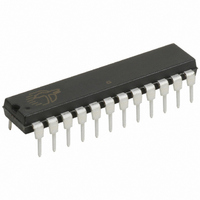
PLDC20G10-25PC Cypress Semiconductor Corp, PLDC20G10-25PC Datasheet - Page 6

PLDC20G10-25PC
Manufacturer Part Number
PLDC20G10-25PC
Description
IC SPLD 10MACROCELL 25NS 24-DIP
Manufacturer
Cypress Semiconductor Corp
Specifications of PLDC20G10-25PC
Programmable Type
SPLD
Number Of Macrocells
10
Voltage - Input
5V
Speed
25ns
Mounting Type
Through Hole
Package / Case
24-DIP (0.300", 7.62mm)
Family Name
PLDC20G10
Process Technology
CMOS
# Macrocells
10
# I/os (max)
10
Propagation Delay Time
25ns
Operating Supply Voltage (typ)
5V
Operating Supply Voltage (min)
4.5V
Operating Supply Voltage (max)
5.5V
Operating Temp Range
0C to 75C
Operating Temperature Classification
Commercial
Mounting
Through Hole
Pin Count
24
Supply Current
55mA
Lead Free Status / RoHS Status
Contains lead / RoHS non-compliant
Other names
428-1284
Available stocks
Company
Part Number
Manufacturer
Quantity
Price
Company:
Part Number:
PLDC20G10-25PC
Manufacturer:
CYP
Quantity:
5 510
Company:
Part Number:
PLDC20G10-25PC
Manufacturer:
TOS
Quantity:
5 510
AC Test Loads and Waveforms (Commercial)
Switching Characteristics
Document #: 38-03010 Rev. **
Equivalent to: THÉVENIN EQUIVALENT (Commercial)
t
t
t
t
t
t
t
t
t
t
t
f
Notes:
Parameter
10. t
11. f
PD
EA
ER
PZX
PXZ
CO
S
H
P
WH
WL
MAX
8.
9.
[10]
Part (a) of AC Test Loads and Waveforms used for all parameters except t
and t
The parameters t
+ 0.5V for an enabled LOW input.
for registered data path operation (no feedback) can be calculated as the greater of (t
guaranteed f
[11]
P
MAX
, minimum guaranteed clock period is that guaranteed for state machine operation and is calculated from t
OUTPUT
, minimum guaranteed operating frequency, is that guaranteed for state machine operation and is calculated from f
PXZ
.
OUTPUT
Input or Feedback to Non-Registered Output
Input to Output Enable
Input to Output Disable
Pin 11 to Output Enable
Pin 11 to Output Disable
Clock to Output
Input or Feedback Set-Up Time
Hold Time
Clock Period
Clock High Time
Clock Low Time
Maximum Frequency
MAX
INCLUDING
JIG AND
SCOPE
ER
for registered data path operation (no feedback) can be calculated as the lower of 1/(t
5V
and t
99
PXZ
are measured as the delay from the input disable logic threshold transition to V
R1 238
(319 MIL)
Description
50pF
Over Operating Range
(a)
2.08V=V
thc
R2 170
(236 MIL)
20G10–15
[3, 8, 9]
ER
OUTPUT
Min. Max. Min. Max. Min. Max. Min. Max.
45.4
, t
12
22
0
8
8
PZX
INCLUDING
JIG AND
SCOPE
B–15
5V
, and t
Equivalent to: THÉVENIN EQUIVALENT (Military/Industrial)
15
15
15
12
12
10
WH
PXZ
+ t
. Part (b) of AC Test Loads and Waveforms used for t
WL
OUTPUT
41.6
12
24
10
10
) or (t
0
B–20
R1 238
(319 MIL)
(b)
S
PLDC20G10B/PLDC20G10
5 pF
Commercial
+ t
20
20
20
15
15
12
WH
H
).
+ t
P
OH
= t
WL
33.3
– 0.5V for an enabled HIGH output or V
S
136
15
30
12
12
) or 1/(t
0
+ t
R2 170
(236 MIL)
–25
CO
. The minimum guaranteed period
MAX
S
25
25
25
20
20
15
+ t
= 1/(t
H
).
18.1
2.13V=V
S
30
55
17
17
0
20G10–14
+ t
–35
CO
). The minimum
35
35
35
25
25
25
thm
20G10–16
Page 6 of 13
ER
MHz
, t
Unit
ns
ns
ns
ns
ns
ns
ns
ns
ns
ns
ns
PZX
OL
,


