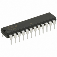
PLDC20G10-25PC Cypress Semiconductor Corp, PLDC20G10-25PC Datasheet

PLDC20G10-25PC
Specifications of PLDC20G10-25PC
Available stocks
Related parts for PLDC20G10-25PC
PLDC20G10-25PC Summary of contents
Page 1
... Note: 1. The CG7C323 is the PLDC20G10 packaged in the JEDEC-compatible 28-pin PLCC pinout. Pin function and pin order is identical for both PLCC pinouts. The difference is in the location of the “no connect” pins. Cypress Semiconductor Corporation Document #: 38-03010 Rev. ** Reprogrammable Logic Device • ...
Page 2
... Preload is important for testing the functionality of the Cypress PLD device. 20G10 Functional Description The PLDC20G10 is a generic 24-pin device that can be pro- grammed to logic functions that include but are not limited to: 20L10, 20L8, 20R8, 20R6, 20R4, 12L10, 14L8, 16L6, 18L4, 20L2, and 20V8 ...
Page 3
... BACK 1 MUX C 3 PIN Product Term OE/Registered/Active LOW 1 Product Term OE/Registered/Active HIGH 0 Product Term OE/Combinatorial/Active LOW 1 Product Term OE/Combinatorial/Active HIGH 0 Pin 13 OE/Registered/Active LOW 1 Pin 13 OE/Registered/Active HIGH 0 Pin 13 OE/Combinatorial/Active LOW 1 Pin 13 OE/Combinatorial/Active HIGH PLDC20G10B/PLDC20G10 OUTPUT ENABLE MUX C 2 20G10–5 Configuration Page ...
Page 4
... Note: 2. Bidirectional I/O configurations are possible only when the combinatorial output option is selected Document #: 38-03010 Rev Figure 2. Product Term OE/Active HIGH Figure 4. Pin 13 OE/Active HIGH [ Figure 6. Product Term OE/Active HIGH Figure 8. Pin 13 OE/Active HIGH PLDC20G10B/PLDC20G10 20G10– 20G10– 20G10– ...
Page 5
... Tested initially and after any design or process changes that may affect these parameters. Document #: 38-03010 Rev Programming Voltage PLDC20G10B and CG7C323B–A ............................... 13.0V PLDC20G10 and CG7C323–A.................................... 14.0V Latch-Up Current..................................................... >200 mA Static Discharge Voltage ............................................. >500V (per MIL-STD-883, Method 8015) ...
Page 6
... B–15 B–20 Min. Max. Min. Max. Min. Max. Min. Max 45.4 41 and t . Part ( Test Loads and Waveforms used for t ER PZX PXZ + PLDC20G10B/PLDC20G10 R2 170 5 pF (236 MIL) 20G10–14 (b) 136 2.13V=V thm 20G10–16 Commercial –25 –35 Unit ...
Page 7
... WL [11] f Maximum Frequency MAX Switching Waveform INPUTS I/O, REGISTERED FEEDBACK REGISTERED OUTPUTS COMBINATORIAL OUTPUTS Document #: 38-03010 Rev (continued) B–20 Min. Max. Min. Max. Min. Max. Min. Max 33 PXZ PLDC20G10B/PLDC20G10 Military/Industrial B–25 –30 – 30.3 25.0 16.6 t PZX t ER Page Unit ns ns ...
Page 8
... OE 0 • • • • • • • • • • • • Document #: 38-03010 Rev PLDC20G10B/PLDC20G10 OUTPUT CELL 23 OUTPUT CELL 22 OUTPUT CELL 21 OUTPUT CELL 20 OUTPUT CELL 19 OUTPUT CELL 18 OUTPUT CELL 17 OUTPUT CELL 16 OUTPUT CELL 15 OUTPUT CELL 14 13 Page ...
Page 9
... (ns) (ns) (ns) (mA) Ordering Code PLDC20G10B–15PC PLDC20G10B–15WC 100 PLDC20G10B–20DMB PLDC20G10–25JC PLDC20G10–25PC/PI PLDC20G10–25WC PLDC20G10–30DMB PLDC20G10–30LMB PLDC20G10–30WMB PLDC20G10–35JC PLDC20G10–35PC MILITARY SPECIFICATIONS Group A Subgroup Testing DC Characteristics Parameter Subgroups Document #: 38-03010 Rev. ** PLDC20G10B/PLDC20G10 Package Name ...
Page 10
... Package Diagrams 24-Lead (300-Mil) CerDIP D14 MIL–STD–1835 D– 9Config.A 28-Square Leadless Chip Carrier L64 MIL–STD–1835 C–4 Document #: 38-03010 Rev. ** PLDC20G10B/PLDC20G10 28-Lead Plastic Leaded Chip Carrier J64 Page ...
Page 11
... Package Diagrams (continued) Document #: 38-03010 Rev. ** 28-Pin Windowed Leaded Chip Carrier H64 PLDC20G10B/PLDC20G10 Page ...
Page 12
... Package Diagrams (continued) Document #: 38-03010 Rev. ** 24-Lead (300-Mil) Molded DIP P13/P13A 24-Lead (300-Mil) Windowed CerDIP W14 MIL–STD–1835 D– 9Config.A PLDC20G10B/PLDC20G10 Page ...
Page 13
... Document Title: PLDC20G10B/PLDC20G10 CMOS Generic 24-Pin Reprogrammable Logic Device Document Number: 38-03010 REV. ECN NO. Issue Date ** 106292 04/25/01 Document #: 38-03010 Rev. ** © Cypress Semiconductor Corporation, 1997. The information contained herein is subject to change without notice. Cypress Semiconductor Corporation assumes no responsibility for the use of any circuitry other than circuitry embodied in a Cypress Semiconductor product ...


