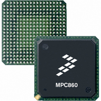
MC68MH360ZP33L Freescale Semiconductor, MC68MH360ZP33L Datasheet - Page 755

MC68MH360ZP33L
Manufacturer Part Number
MC68MH360ZP33L
Description
IC MPU 32BIT QUICC 357-PBGA
Manufacturer
Freescale Semiconductor
Specifications of MC68MH360ZP33L
Processor Type
M683xx 32-Bit
Speed
33MHz
Voltage
5V
Mounting Type
Surface Mount
Package / Case
357-PBGA
Lead Free Status / RoHS Status
Contains lead / RoHS non-compliant
Features
-
Available stocks
Company
Part Number
Manufacturer
Quantity
Price
Company:
Part Number:
MC68MH360ZP33L
Manufacturer:
FREESCALE
Quantity:
1 831
Company:
Part Number:
MC68MH360ZP33L
Manufacturer:
MOTOLOLA
Quantity:
672
Company:
Part Number:
MC68MH360ZP33L
Manufacturer:
Freescale Semiconductor
Quantity:
10 000
Part Number:
MC68MH360ZP33L
Manufacturer:
FREESCALE
Quantity:
20 000
Company:
Part Number:
MC68MH360ZP33LR2
Manufacturer:
Freescale Semiconductor
Quantity:
10 000
- Current page: 755 of 962
- Download datasheet (5Mb)
In addition, the QUICC allows the IOUT2–IOUT0 pins to be generated in two different ways:
at the expense of parity pins or at the expense of some interrupt requests. In this application,
parity is used with some of the external memories; thus, three of the interrupt inputs are sac-
rificed.
Once the MC68EC040 recognizes the interrupt, it responds with an interrupt acknowledge
cycle. The QUICC recognizes the MC68EC040 interrupt acknowledge cycle using the
address pins, TT1–TT0 pins (they are both high), and the TM2–TM0 pins (which output the
inverse of the value on IPL2–IPL0). If the source of the interrupt is the CPM, the periodic
interrupt timer, or the software watchdog, the QUICC responds by placing the vector on the
bus. If the source of the interrupt is an IRQx pin, the QUICC then responds by outputting the
AVECO signal to the MC68EC040, depending on what was programmed into the autovector
register in the SIM60.
When the QUICC is in slave mode, what is normally the AVEC pin (an input) becomes the
AVECO pin (an output) for use with external processors.
9.4.1.5 BUS ARBITRATION. When the QUICC is configured to MC68040 companion
mode, the QUICC bus arbitration pins are configured to directly interface to those of the
MC68EC040. The QUICC bus request (BR) is an input from the MC68EC040, and the
QUICC bus grant (BG) is an output to the MC68EC040. The QUICC also has a bus busy
(BB) function to match that of the MC68EC040.
The MC68EC040 LOCK pin can be connected to the QUICC to allow MC68EC040 locked
cycles to continue without interruption from the QUICC. The CONFIG0 pin on the QUICC
becomes the LOCK input to the QUICC after system reset when the QUICC is in MC68040
companion mode. Since the MC68EC040 LOCK pin is inactive high, it may be connected
directly to the QUICC LOCK pin with a pullup resistor.
The BR input from the MC68EC040 is not the highest priority in this system. The SDMA
channels have a higher priority. Thus, the BCLRO function of the QUICC is not used in this
design because it is not needed.
The QUICC also has a BCLRI signal that allows internal masters to be cleared off the bus.
This pin can be used with the MC68EC040 IPEND pin to give the MC68EC040 interrupts
priority over the QUICC internal masters. This function is not implemented in the design for
the sake of simplicity and use of the alternate function of the pin, the RAS1DD function.
However, if it were implemented, the IPEND signal from the MC68EC040 would have to be
latched and kept low by the MC68EC040 until completion of the interrupt routine. (If it was
not latched, the QUICC could take the bus back from the MC68EC040 as soon as the inter-
MOTOROLA
If the MC68040 were used rather than the MC68EC040, the
IPL2–IPL0 pins take on meanings during reset to determine the
buffer strength. Thus, additional logic may be required during re-
set to select the desired buffer strength of the MC68040. This
logic does not exist on the MC68EC040 (except on very early
versions of that device).
Freescale Semiconductor, Inc.
For More Information On This Product,
MC68360 USER’S MANUAL
Go to: www.freescale.com
NOTE
Applications
9-35
Related parts for MC68MH360ZP33L
Image
Part Number
Description
Manufacturer
Datasheet
Request
R
Part Number:
Description:
Manufacturer:
Freescale Semiconductor, Inc
Datasheet:
Part Number:
Description:
Manufacturer:
Freescale Semiconductor, Inc
Datasheet:
Part Number:
Description:
Manufacturer:
Freescale Semiconductor, Inc
Datasheet:
Part Number:
Description:
Manufacturer:
Freescale Semiconductor, Inc
Datasheet:
Part Number:
Description:
Manufacturer:
Freescale Semiconductor, Inc
Datasheet:
Part Number:
Description:
Manufacturer:
Freescale Semiconductor, Inc
Datasheet:
Part Number:
Description:
Manufacturer:
Freescale Semiconductor, Inc
Datasheet:
Part Number:
Description:
Manufacturer:
Freescale Semiconductor, Inc
Datasheet:
Part Number:
Description:
Manufacturer:
Freescale Semiconductor, Inc
Datasheet:
Part Number:
Description:
Manufacturer:
Freescale Semiconductor, Inc
Datasheet:
Part Number:
Description:
Manufacturer:
Freescale Semiconductor, Inc
Datasheet:
Part Number:
Description:
Manufacturer:
Freescale Semiconductor, Inc
Datasheet:
Part Number:
Description:
Manufacturer:
Freescale Semiconductor, Inc
Datasheet:
Part Number:
Description:
Manufacturer:
Freescale Semiconductor, Inc
Datasheet:
Part Number:
Description:
Manufacturer:
Freescale Semiconductor, Inc
Datasheet:


