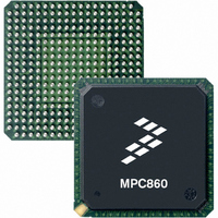
MC68MH360ZP33L Freescale Semiconductor, MC68MH360ZP33L Datasheet - Page 512

MC68MH360ZP33L
Manufacturer Part Number
MC68MH360ZP33L
Description
IC MPU 32BIT QUICC 357-PBGA
Manufacturer
Freescale Semiconductor
Specifications of MC68MH360ZP33L
Processor Type
M683xx 32-Bit
Speed
33MHz
Voltage
5V
Mounting Type
Surface Mount
Package / Case
357-PBGA
Lead Free Status / RoHS Status
Contains lead / RoHS non-compliant
Features
-
Available stocks
Company
Part Number
Manufacturer
Quantity
Price
Company:
Part Number:
MC68MH360ZP33L
Manufacturer:
FREESCALE
Quantity:
1 831
Company:
Part Number:
MC68MH360ZP33L
Manufacturer:
MOTOLOLA
Quantity:
672
Company:
Part Number:
MC68MH360ZP33L
Manufacturer:
Freescale Semiconductor
Quantity:
10 000
Part Number:
MC68MH360ZP33L
Manufacturer:
FREESCALE
Quantity:
20 000
Company:
Part Number:
MC68MH360ZP33LR2
Manufacturer:
Freescale Semiconductor
Quantity:
10 000
- Current page: 512 of 962
- Download datasheet (5Mb)
Serial Communication Controllers (SCCs)
7-188
5. Connect the CLK7 pin to SCC4 using the SI. Write the R4CS bits in SICR to 110.
6. Connect the SCC4 to the NMSI (i.e., its own set of pins). Clear the SC4 bit
7. Write $0740 to the SDCR to initialize the SDMA Configuration Register.
8. Write RBASE and TBASE in the SCC parameter RAM to point to the Rx BD and Tx
9. Program the CR to execute the INIT RX & TX PARAMS command for this channel."
10. Write RFCR with $18 and TFCR with $18 for normal operation.
11. Write MRBLR with the maximum number of bytes per receive buffer. For this case,
12. Write C_MASK with $0000F0B8 to comply with 16-bit CCITT-CRC.
13. Write C_PRES with $0000FFFF to comply with 16-bit CCITT-CRC.
14. Clear DISFC, CRCEC, ABTSC, NMARC, and RETRC for the sake of clarity.
15. Write MFLR with $0100 to make the maximum frame size 256 bytes.
16. Write RFTHR with $0001 to allow interrupts after each frame.
17. Write HMASK with $0000 to allow all addresses to be recognized.
18. Clear HADDR1, HADDR2, HADDR3, and HADDR4 for clarity.
19. Initialize the Rx BD. Assume the Rx data buffer is at $00001000 in main memory.
20. Initialize the Tx BD. Assume the Tx data frame is at $00002000 in main memory
21. Write $FFFF to the SCCE to clear any previous events.
22. Write $001A to the SCCM to enable the TXE, RXF, and TXB interrupts.
23. Write $08000000 to the CIMR to allow SCC4 to generate a system interrupt. (The
24. Write $00000000 to GSMR_H4 to enable normal behavior of the CTS and CD pins
25. Write $00000000 to GSMR_L4 to configure the CTS and CD pins to automatically
Write the T4CS bits in SICR to 110.
in the SICR.
BDs in the dual-port RAM. Assuming one Rx BD at the beginning of dual-port RAM
and one Tx BD following that Rx BD, write RBASE with $0000 and TBASE with
$0008.
For instance, to execute this command for SCC1, write $0001 to the CR. This com-
mand causes the RBPTR and TBPTR parameters of the serial channel to be updated
with the new values just programmed into RBASE and TBASE.
assume 256 bytes, so MRBLR = $0100. The value 256 was chosen to allow an
entire receive frame to fit into one receive buffer (see MFLR below).
Write $B000 to Rx_BD_Status. Write $0000 to Rx_BD_Length (not required—done
for instructional purposes only). Write $00001000 to Rx_BD_Pointer.
and contains five 8-bit characters. Write $BC00 to Tx_BD_Status. Write $0005 to
Tx_BD_Length. Write $00002000 to Tx_BD_Pointer.
CICR should also be initialized.)
and idles between frames (as opposed to flags).
control transmission and reception (DIAG bits) and the HDLC mode. Normal
operation of the transmit clock is used (TCI is cleared). Notice that the transmitter
(ENT) and receiver (ENR) have not been enabled. If inverted HDLC operation
Freescale Semiconductor, Inc.
For More Information On This Product,
MC68360 USER’S MANUAL
Go to: www.freescale.com
MOTOROLA
Related parts for MC68MH360ZP33L
Image
Part Number
Description
Manufacturer
Datasheet
Request
R
Part Number:
Description:
Manufacturer:
Freescale Semiconductor, Inc
Datasheet:
Part Number:
Description:
Manufacturer:
Freescale Semiconductor, Inc
Datasheet:
Part Number:
Description:
Manufacturer:
Freescale Semiconductor, Inc
Datasheet:
Part Number:
Description:
Manufacturer:
Freescale Semiconductor, Inc
Datasheet:
Part Number:
Description:
Manufacturer:
Freescale Semiconductor, Inc
Datasheet:
Part Number:
Description:
Manufacturer:
Freescale Semiconductor, Inc
Datasheet:
Part Number:
Description:
Manufacturer:
Freescale Semiconductor, Inc
Datasheet:
Part Number:
Description:
Manufacturer:
Freescale Semiconductor, Inc
Datasheet:
Part Number:
Description:
Manufacturer:
Freescale Semiconductor, Inc
Datasheet:
Part Number:
Description:
Manufacturer:
Freescale Semiconductor, Inc
Datasheet:
Part Number:
Description:
Manufacturer:
Freescale Semiconductor, Inc
Datasheet:
Part Number:
Description:
Manufacturer:
Freescale Semiconductor, Inc
Datasheet:
Part Number:
Description:
Manufacturer:
Freescale Semiconductor, Inc
Datasheet:
Part Number:
Description:
Manufacturer:
Freescale Semiconductor, Inc
Datasheet:
Part Number:
Description:
Manufacturer:
Freescale Semiconductor, Inc
Datasheet:


