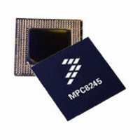
MPC8245LZU333D Freescale Semiconductor, MPC8245LZU333D Datasheet - Page 45

MPC8245LZU333D
Manufacturer Part Number
MPC8245LZU333D
Description
IC MPU 32BIT 333MHZ 352-TBGA
Manufacturer
Freescale Semiconductor
Series
PowerQUICC IIr
Specifications of MPC8245LZU333D
Processor Type
MPC82xx PowerQUICC II 32-bit
Speed
333MHz
Voltage
2V
Mounting Type
Surface Mount
Package / Case
352-TBGA
Core Size
32 Bit
Program Memory Size
32KB
Cpu Speed
333MHz
Embedded Interface Type
I2C
Digital Ic Case Style
TBGA
No. Of Pins
352
Supply Voltage Range
1.9V To 2.2V
Rohs Compliant
No
Family Name
MPC82XX
Device Core
PowerPC
Device Core Size
64b
Frequency (max)
333MHz
Instruction Set Architecture
RISC
Supply Voltage 1 (typ)
2/2.1/3.3V
Operating Supply Voltage (max)
2.2/3.465V
Operating Supply Voltage (min)
1.9/3.135V
Operating Temp Range
0C to 105C
Operating Temperature Classification
Commercial
Mounting
Surface Mount
Pin Count
352
Package Type
TBGA
Lead Free Status / RoHS Status
Contains lead / RoHS non-compliant
Features
-
Lead Free Status / Rohs Status
Not Compliant
Available stocks
Company
Part Number
Manufacturer
Quantity
Price
Company:
Part Number:
MPC8245LZU333D
Manufacturer:
FREE
Quantity:
12
Company:
Part Number:
MPC8245LZU333D
Manufacturer:
MOTOROLA
Quantity:
648
Company:
Part Number:
MPC8245LZU333D
Manufacturer:
Freescale Semiconductor
Quantity:
10 000
Part Number:
MPC8245LZU333D
Manufacturer:
MOTOROLA/摩托罗拉
Quantity:
20 000
7.3
To ensure reliable operation, connect unused inputs to an appropriate signal level. Tie unused active-low
inputs to OV
Power and ground connections must be made to all external V
The PCI_SYNC_OUT signal is to be routed halfway out to the PCI devices and returned to the
PCI_SYNC_IN input of the MPC8245.
The SDRAM_SYNC_OUT signal is to be routed halfway out to the SDRAM devices and then returned to
the SDRAM_SYNC_IN input of the MPC8245. The trace length can be used to skew or adjust the timing
window as needed. See the Tundra Tsi107™ Design Guide (AN1849) and Freescale application notes
AN2164, MPC8245/MPC8241 Memory Clock Design Guidelines: Part 1 and AN2746,
MPC8245/MPC8241 Memory Clock Design Guidelines: Part 2 for details. Note that there is an
SDRAM_SYNC_IN to PCI_SYNC_IN time requirement (refer to
specifications).
7.4
The data bus input receivers are normally turned off when no read operation is in progress; therefore, they
do not require pull-up resistors on the bus. The data bus signals are: MDH[0:31], MDL[0:31], and
PAR[0:7].
If the 32-bit data bus mode is selected, the input receivers of the unused data and parity bits (MDL[0:31]
and PAR[4:7]) are disabled, and their outputs drive logic zeros when they would otherwise normally be
driven. For this mode, these pins do not require pull-up resistors and should be left unconnected to
minimize possible output switching.
The TEST0 pin requires a pull-up resistor of 120 Ω or less connected to OV
RTC should have weak pull-up resistors (2–10 kΩ) connected to GV
The following signals should be pulled up to OV
SMI, SRESET/SDMA12, TBEN/SDMA13, CHKSTOP_IN/SDMA14, TRIG_IN/RCS2, INTA,
QACK/DA0 and DRDY. Note that QACK/DA0 should be left without a pull-up resistor only if an external
clock is used because this signal enables internal clock flipping logic when it is low on reset, which is
necessary when the PLL[0:4] signals select a half-clock frequency ratio and an external PLL is used to
drive the SDRAM device.
It is recommended that the following PCI control signals be pulled up to LV
weak pull-up resistors (2–10 kΩ): DEVSEL, FRAME, IRDY, LOCK, PERR, SERR, STOP, and TRDY.
The resistor values may need to be adjusted stronger to reduce induced noise on specific board designs.
The following pins have internal pull-up resistors enabled at all times: REQ[3:0], REQ4/DA4, TCK, TDI,
TMS, and TRST. See
The following pins have internal pull-up resistors enabled only while device is in the reset state:
GNT4/DA5, MDL0, FOE, RCS0, SDRAS, SDCAS, CKE, AS, MCP, MAA[0:2], and PMAA[0:2]. See
Table
Freescale Semiconductor
16.
Connection Recommendations
Pull-Up/Pull-Down Resistor Requirements
DD
. Connect unused active-high inputs tie to GND. All NC signals must remain unconnected.
Table
MPC8245 Integrated Processor Hardware Specifications, Rev. 10
16.
DD
with weak pull-up resistors (2–10 kΩ): SDA, SCL,
DD
, OV
Table 10
DD
DD
.
, GV
DD
for the input AC timing
DD
(the clamping voltage) with
DD
.
, LV
DD
, and GND pins.
System Design
45


