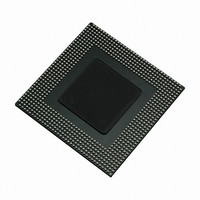
MPC8360EVVAJDGA Freescale Semiconductor, MPC8360EVVAJDGA Datasheet - Page 87

MPC8360EVVAJDGA
Manufacturer Part Number
MPC8360EVVAJDGA
Description
IC MPU POWERQUICC II PRO 740TBGA
Manufacturer
Freescale Semiconductor
Series
PowerQUICC II PROr
Specifications of MPC8360EVVAJDGA
Processor Type
MPC83xx PowerQUICC II Pro 32-Bit
Speed
533MHz
Voltage
1.2V
Mounting Type
Surface Mount
Package / Case
740-TBGA
Processor Series
MPC8xxx
Core
e300
Data Bus Width
32 bit
Development Tools By Supplier
MPC8360E-RDK
Maximum Clock Frequency
533 MHz
Maximum Operating Temperature
+ 105 C
Mounting Style
SMD/SMT
I/o Voltage
1.8 V, 2.5 V, 3.3 V
Minimum Operating Temperature
0 C
Core Size
32 Bit
Program Memory Size
64KB
Cpu Speed
533MHz
Embedded Interface Type
I2C, SPI, USB, UART
Digital Ic Case Style
TBGA
No. Of Pins
740
Rohs Compliant
Yes
For Use With
MPC8360EA-MDS-PB - KIT APPLICATION DEV 8360 SYSTEMMPC8360E-RDK - BOARD REFERENCE DESIGN FOR MPC
Lead Free Status / RoHS Status
Lead free / RoHS Compliant
Features
-
Lead Free Status / Rohs Status
Lead free / RoHS Compliant
Available stocks
Company
Part Number
Manufacturer
Quantity
Price
Company:
Part Number:
MPC8360EVVAJDGA
Manufacturer:
Freescale Semiconductor
Quantity:
135
Company:
Part Number:
MPC8360EVVAJDGA
Manufacturer:
Freescale Semiconductor
Quantity:
10 000
Part Number:
MPC8360EVVAJDGA
Manufacturer:
FREESCALE
Quantity:
20 000
PCI_SYNC_OUT is connected externally to PCI_SYNC_IN to allow the internal clock subystem to
synchronize to the system PCI clocks. PCI_SYNC_OUT must be connected properly to PCI_SYNC_IN,
with equal delay to all PCI agent devices in the system, to allow the device to function. When the device
is configured as a PCI agent device, PCI_CLK is the primary input clock. When the device is configured
as a PCI agent device the CLKIN and the CFG_CLKIN_DIV signals should be tied to GND.
When the device is configured as a PCI host device (RCWH[PCIHOST] = 1) and PCI clock output is
disabled (RCWH[PCICKDRV] = 0), clock distribution and balancing done externally on the board.
Therefore, PCI_SYNC_IN is the primary input clock.
As shown in
Engine block phase-locked loop (PLL), the system PLL, and the clock unit to create the QUICC Engine
clock (ce_clk), the coherent system bus clock (csb_clk), the internal DDRC1 controller clock (ddr1_clk),
and the internal clock for the local bus interface unit and DDR2 memory controller (lb_clk).
The csb_clk frequency is derived from a complex set of factors that can be simplified into the following
equation:
In PCI host mode, PCI_SYNC_IN × (1 + CFG_CLKIN_DIV) is the CLKIN frequency; in PCI agent
mode, CFG_CLKIN_DIV must be pulled down (low), so PCI_SYNC_IN × (1 + CFG_CLKIN_DIV) is
the PCI_CLK frequency.
The csb_clk serves as the clock input to the e300 core. A second PLL inside the e300 core multiplies up
the csb_clk frequency to create the internal clock for the e300 core (core_clk). The system and core PLL
multipliers are selected by the SPMF and COREPLL fields in the reset configuration word low (RCWL)
which is loaded at power-on reset or by one of the hard-coded reset options. See Chapter 4, “Reset,
Clocking, and Initialization,” in the MPC8360E PowerQUICC II Pro Integrated Communications
Processor Family Reference Manual for more information on the clock subsystem.
The ce_clk frequency is determined by the QUICC Engine PLL multiplication factor (RCWL[CEPMF)
and the QUICC Engine PLL division factor (RCWL[CEPDF]) according to the following equation:
The internal ddr1_clk frequency is determined by the following equation:
Note that the lb_clk clock frequency (for DDRC2) is determined by RCWL[LBCM]. The internal
ddr1_clk frequency is not the external memory bus frequency; ddr1_clk passes through the DDRC1 clock
divider (÷2) to create the differential DDRC1 memory bus clock outputs (MEMC1_MCK and
MEMC1_MCK). However, the data rate is the same frequency as ddr1_clk.
The internal lb_clk frequency is determined by the following equation:
Note that lb_clk is not the external local bus or DDRC2 frequency; lb_clk passes through the a LB clock
divider to create the external local bus clock outputs (LSYNC_OUT and LCLK[0:2]). The LB clock
divider ratio is controlled by LCRR[CLKDIV].
Freescale Semiconductor
MPC8360E/MPC8358E PowerQUICC II Pro Processor Revision 2.x TBGA Silicon Hardware Specifications, Rev. 4
csb_clk = {PCI_SYNC_IN × (1 + CFG_CLKIN_DIV)} × SPMF
ce_clk = (primary clock input × CEPMF) ÷ (1 + CEPDF)
ddr1_clk = csb_clk × (1 + RCWL[DDR1CM])
lb_clk = csb_clk × (1 + RCWL[LBCM])
Figure 54
and
Figure
55, the primary clock input (frequency) is multiplied by the QUICC
Clocking
87


