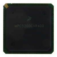
MPC5200CVR400 Freescale Semiconductor, MPC5200CVR400 Datasheet - Page 48

MPC5200CVR400
Manufacturer Part Number
MPC5200CVR400
Description
IC MPU 32BIT 400MHZ PPC 272-PBGA
Manufacturer
Freescale Semiconductor
Datasheet
1.MPC5200CVR400B.pdf
(80 pages)
Specifications of MPC5200CVR400
Processor Type
MPC52xx PowerPC 32-Bit
Speed
400MHz
Voltage
1.5V
Mounting Type
Surface Mount
Package / Case
272-PBGA
Family Name
MPC52xx
Device Core
PowerPC
Device Core Size
32b
Frequency (max)
400MHz
Instruction Set Architecture
RISC
Operating Supply Voltage (max)
1.58V
Operating Supply Voltage (min)
1.42V
Operating Temp Range
-40C to 85C
Operating Temperature Classification
Industrial
Mounting
Surface Mount
Pin Count
272
Package Type
BGA
Lead Free Status / RoHS Status
Lead free / RoHS Compliant
Features
-
Lead Free Status / Rohs Status
Compliant
Available stocks
Company
Part Number
Manufacturer
Quantity
Price
Company:
Part Number:
MPC5200CVR400
Manufacturer:
FREESCAL
Quantity:
200
Company:
Part Number:
MPC5200CVR400
Manufacturer:
Freescale Semiconductor
Quantity:
10 000
Company:
Part Number:
MPC5200CVR400B
Manufacturer:
Marvell
Quantity:
1 001
Company:
Part Number:
MPC5200CVR400B
Manufacturer:
FREESCAL
Quantity:
200
Company:
Part Number:
MPC5200CVR400B
Manufacturer:
Freescale Semiconductor
Quantity:
10 000
Part Number:
MPC5200CVR400B
Manufacturer:
FREESCALE
Quantity:
20 000
Company:
Part Number:
MPC5200CVR400BM62C
Manufacturer:
FRRESCAL..
Quantity:
2 831
Electrical and Thermal Characteristics
48
(CLKPOL=0)
NOTES:
1
(CLKPOL=1)
Inter Peripheral Clock is defined in the MPC5200 User Manual [1].
Sym
1
2
3
4
5
6
7
8
9
Output
Output
Output
Output
MOSI
MISO
SCK
Input
SCK
Cycle time
Clock high or low time
Slave select clock delay
Output Data valid after Slave Select (SS)
Output Data valid after SCK
Input Data setup time
Input Data hold time
Slave disable lag time
Sequential Transfer delay
SS
Table 37. Timing Specifications — SPI Slave Mode, Format 0 (CPHA = 0)
Figure 33. Timing Diagram — SPI Master Mode, Format 0 (CPHA = 0)
4
Output timing was specified at a nominal 50 pF load.
6
3
Description
2
5
7
MPC5200 Data Sheet, Rev. 4
1
6
2
NOTE
10
11
7
15.0
15.0
50.0
Min
0.0
—
—
4
2
1
10
11
1024
Max
50.0
50.0
512
—
—
—
—
—
8
IP-Bus Cycle
IP-Bus Cycle
IP-Bus Cycle
Units
ns
ns
ns
ns
ns
ns
Freescale Semiconductor
9
1
1
1
SpecID
A11.12
A11.13
A11.14
A11.15
A11.16
A11.17
A11.18
A11.19
A11.20


