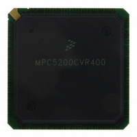
MPC5200CVR400 Freescale Semiconductor, MPC5200CVR400 Datasheet - Page 30

MPC5200CVR400
Manufacturer Part Number
MPC5200CVR400
Description
IC MPU 32BIT 400MHZ PPC 272-PBGA
Manufacturer
Freescale Semiconductor
Datasheet
1.MPC5200CVR400B.pdf
(80 pages)
Specifications of MPC5200CVR400
Processor Type
MPC52xx PowerPC 32-Bit
Speed
400MHz
Voltage
1.5V
Mounting Type
Surface Mount
Package / Case
272-PBGA
Family Name
MPC52xx
Device Core
PowerPC
Device Core Size
32b
Frequency (max)
400MHz
Instruction Set Architecture
RISC
Operating Supply Voltage (max)
1.58V
Operating Supply Voltage (min)
1.42V
Operating Temp Range
-40C to 85C
Operating Temperature Classification
Industrial
Mounting
Surface Mount
Pin Count
272
Package Type
BGA
Lead Free Status / RoHS Status
Lead free / RoHS Compliant
Features
-
Lead Free Status / Rohs Status
Compliant
Available stocks
Company
Part Number
Manufacturer
Quantity
Price
Company:
Part Number:
MPC5200CVR400
Manufacturer:
FREESCAL
Quantity:
200
Company:
Part Number:
MPC5200CVR400
Manufacturer:
Freescale Semiconductor
Quantity:
10 000
Company:
Part Number:
MPC5200CVR400B
Manufacturer:
Marvell
Quantity:
1 001
Company:
Part Number:
MPC5200CVR400B
Manufacturer:
FREESCAL
Quantity:
200
Company:
Part Number:
MPC5200CVR400B
Manufacturer:
Freescale Semiconductor
Quantity:
10 000
Part Number:
MPC5200CVR400B
Manufacturer:
FREESCALE
Quantity:
20 000
Company:
Part Number:
MPC5200CVR400BM62C
Manufacturer:
FRRESCAL..
Quantity:
2 831
Electrical and Thermal Characteristics
3.3.7.2
NOTES:
1. Wait States (WS) can be programmed in the Chip Select X Register, Bit field WaitP and WaitX. It can be specified 0 - 65535.
2. Example:
3. ACK is output and indicates the burst.
30
Long Burst is used, this means the CS related BERx and SLB bits of the Chip Select Burst Control Register are set and a
burst on the internal XLB is executed. => LB = 1
Data bus width is 8 bit. => DS = 8
=> 4
Wait State is set to 10. => WS = 10
1+10+32 = 43 => CS is asserted for 43 PCI cycles.
Sym
t
t
CSN
CSA
t
t
t
t
t
t
t
t
t
t
t
t
t
t
t
10
11
12
13
14
15
3
4
5
6
7
8
9
1
2
1
*2*(32/8) = 32 => ACK is asserted for 32 PCI cycles to transfer one cache line.
PCI CLK to CS assertion
PCI CLK to CS negation
CS pulse width
ADDR valid before CS assertion
ADDR hold after CS negation
OE assertion before CS assertion
OE negation before CS negation
RW valid before CS assertion
RW hold after CS negation
DATA setup before rising edge of
PCI
DATA hold after rising edge of PCI
DATA hold after CS negation
ACK assertion after CS assertion
ACK negation before CS negation
ACK pulse width
CS assertion after TS assertion
TS pulse width
Burst Mode
Description
Table 25. Burst Mode Timing
MPC5200 Data Sheet, Rev. 4
(1+WS+4
4
LB
*2*(32/DS)*t
t
t
t
t
t
LB
IPBIck
PCIck
PCIck
PCIck
PCIck
Min
1.8
0
0
-
-
-
-
-
*2*(32/DS))*
-
-
-
PCIck
(1+WS+4
4
LB
(WS+1)*t
(DC+1)*t
*2*(32/DS)*t
*t
t
t
Max
LB
PCIck
PCIck
-0.7
1.8
1.8
PCIck
0.8
0.4
0.4
0.6
-
-
-
-
*2*(32/DS))
PCIck
PCIck
PCIck
Units Notes SpecID
ns
ns
ns
ns
ns
ns
ns
ns
ns
ns
ns
ns
ns
ns
ns
ns
ns
Freescale Semiconductor
1,2
2,3
3
A7.20
A7.21
A7.24
A7.22
A7.23
A7.25
A7.26
A7.27
A7.28
A7.29
A7.30
A7.31
A7.32
A7.33
A7.34
A7.35
A7.36


