CY7C63743-SXC Cypress Semiconductor Corp, CY7C63743-SXC Datasheet - Page 27
CY7C63743-SXC
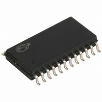
Manufacturer Part Number
CY7C63743-SXC
Description
IC MCU 8K USB/PS2 LS 24SOIC
Manufacturer
Cypress Semiconductor Corp
Series
enCoRe™r
Specifications of CY7C63743-SXC
Applications
USB Microcontroller
Core Processor
M8B
Program Memory Type
OTP (8 kB)
Controller Series
CY7C637xx
Ram Size
256 x 8
Interface
PS2, USB
Number Of I /o
16
Voltage - Supply
4 V ~ 5.5 V
Operating Temperature
0°C ~ 70°C
Mounting Type
Surface Mount
Package / Case
24-SOIC (7.5mm Width)
Lead Free Status / RoHS Status
Lead free / RoHS Compliant
Other names
428-1622
Available stocks
Company
Part Number
Manufacturer
Quantity
Price

Part Number:
CY7C63743-SXC
Manufacturer:
CYPRESS/赛普拉斯
Quantity:
20 000


20.0
Bit 7: IRQ Pending
Bit 6: Watchdog Reset
Bit 5: Bus Interrupt Event
Bit 4: LVR/BOR Reset
Document #: 38-08022 Rev. *B
Read/Write
Bit Name
When an interrupt is generated, it is registered as a pending
interrupt. The interrupt will remain pending until its interrupt
enable bit is set (Figure 21-1 and Figure 21-2) and inter-
rupts are globally enabled (Bit 2, Processor Status and
Control Register). At that point the internal interrupt han-
dling sequence will clear the IRQ Pending bit until another
interrupt is detected as pending. This bit is only valid if the
Global Interrupt Enable bit is disabled.
1 = There are pending interrupts.
0 = No pending interrupts.
The Watchdog Timer Reset (WDR) occurs when the inter-
nal Watchdog timer rolls over. The timer will roll over and
WDR will occur if it is not cleared within t
26.0 for the value of t
LVR/BOR. Note that a Watchdog reset can occur with a
POR/LVR/BOR event, as discussed at the end of this sec-
tion.
1 = A Watchdog reset occurs.
0 = No Watchdog reset
The Bus Reset Status is set whenever the event for the
USB Bus Reset or PS/2 Activity interrupt occurs. The event
type (USB or PS/2) is selected by the state of the USB-PS/2
Interrupt Mode bit in the USB Status and Control Register
(see Figure 13-1). The details on the event conditions that
set this bit are given in Section 21.3. In either mode, this bit
is set as soon as the event has lasted for 128–256 µs, and
the bit will be set even if the interrupt is not enabled. The bit
is only cleared by firmware or LVR/WDR.
1 = A USB reset occurred or PS/2 Activity is detected, de-
pending on USB-PS/2 Interrupt Select bit.
0 = No event detected since last cleared by firmware or
LVR/WDR.
The Low-voltage or Brown-out Reset is set to ‘1’ during a
power-on reset. Firmware can check bits 4 and 6 in the
reset handler to determine whether a reset was caused by
a LVR/BOR condition or a Watchdog timeout. This bit is not
affected by WDR. Note that a LVR/BOR event may be fol-
lowed by a Watchdog reset before firmware begins execut-
ing, as explained at the end of this section.
1 = A POR or LVR has occurred.
0 = No POR nor LVR since this bit last cleared.
Reset
Bit #
Processor Status and Control Register
Pending
IRQ
R
7
0
WATCH
Figure 20-1. Processor Status and Control Register (Address 0xFF)
Watchdog
Reset
). This bit is cleared by an
R/W
6
1
FOR
FOR
WATCH
Interrupt
Event
R/W
Bus
5
0
(see Section
LVR/BOR
Reset
R/W
4
1
Bit 3: Suspend
Bit 2: Interrupt Enable Sense
Bit 1: Reserved. Must be written as a 0.
Bit 0: Run
During power-up, or during a low-voltage reset, the Processor
Status and Control Register is set to 00010001, which
indicates a LVR/BOR (bit 4 set) has occurred and no interrupts
are pending (bit 7 clear). Note that during the t
suspend at start-up (explained in Section 10.1), a Watchdog
Reset will also occur. When a WDR occurs during the
power-up suspend interval, firmware would read 01010001
from the Status and Control Register after power-up. Normally
the LVR/BOR bit should be cleared so that a subsequent WDR
can be clearly identified. Note that if a USB bus reset (long
SE0) is received before firmware examines this register, the
Bus Interrupt Event bit would also be set.
Writing a '1' to the Suspend bit will halt the processor and
cause the microcontroller to enter the suspend mode that
significantly reduces power consumption. An interrupt or
USB bus activity will cause the device to come out of sus-
pend. After coming out of suspend, the device will resume
firmware execution at the instruction following the IOWR
which put the part into suspend. When writing the suspend
bit with a resume condition present (such as non-idle USB
activity), the suspend state will still be entered, followed
immediately by the wake-up process (with appropriate de-
lays for the clock start-up). See Section 11.0 for more de-
tails on suspend mode operation.
1 = Suspend the processor.
0 = Not in suspend mode. Cleared by the hardware when
resuming from suspend.
This bit shows whether interrupts are enabled or disabled.
Firmware has no direct control over this bit as writing a zero
or one to this bit position will have no effect on interrupts.
This bit is further gated with the bit settings of the Global
Interrupt Enable Register (Figure 21-1) and USB Endpoint
Interrupt Enable Register (Figure 21-2). Instructions DI, EI,
and RETI manipulate the state of this bit.
1 = Interrupts are enabled.
0 = Interrupts are masked off.
This bit is manipulated by the HALT instruction. When Halt
is executed, the processor clears the run bit and halts at the
end of the current instruction. The processor remains halt-
ed until a reset occurs (low-voltage, brown-out, or Watch-
dog). This bit should normally be written as a ‘1’.
Suspend
R/W
3
0
Interrupt
Enable
Sense
R
2
0
Reserved
1
0
-
CY7C63722
CY7C63723
CY7C63743
START
Page 27 of 49
ms partial
Run
R/W
0
1
Related parts for CY7C63743-SXC
Image
Part Number
Description
Manufacturer
Datasheet
Request
R

Part Number:
Description:
Manufacturer:
Cypress Semiconductor Corp
Datasheet:
Part Number:
Description:
Manufacturer:
Cypress Semiconductor Corp
Datasheet:
Part Number:
Description:
Manufacturer:
Cypress Semiconductor Corp
Datasheet:
Part Number:
Description:
Manufacturer:
Cypress Semiconductor Corp
Datasheet:
Part Number:
Description:
Manufacturer:
Cypress Semiconductor Corp
Datasheet: