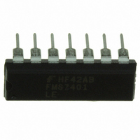
FMS7401LEN14 Fairchild Semiconductor, FMS7401LEN14 Datasheet - Page 13

FMS7401LEN14
Manufacturer Part Number
FMS7401LEN14
Description
IC CTRLR POWER DGTL EEPROM 14DIP
Manufacturer
Fairchild Semiconductor
Datasheet
1.FMS7401LVN.pdf
(81 pages)
Specifications of FMS7401LEN14
Applications
Digital Power Controller
Core Processor
8-Bit
Program Memory Type
EEPROM (1 kB)
Ram Size
64 x 8
Number Of I /o
8
Voltage - Supply
2.7 V ~ 3.6 V
Operating Temperature
-40°C ~ 85°C
Mounting Type
Through Hole
Package / Case
14-DIP (0.300", 7.62mm)
Output Current
5 mA
Input Voltage
2.7 V to 3.6 V
Switching Frequency
2 MHz
Operating Temperature Range
- 40 C to + 85 C
Mounting Style
Through Hole
Lead Free Status / RoHS Status
Lead free / RoHS Compliant
Interface
-
Controller Series
-
Lead Free Status / Rohs Status
Lead free / RoHS Compliant
Other names
FMS7401LEN14_NL
FMS7401LEN14_NL
FMS7401LEN14_NL
Available stocks
Company
Part Number
Manufacturer
Quantity
Price
Company:
Part Number:
FMS7401LEN14
Manufacturer:
Rohm
Quantity:
21 626
3
The FMS7401L has both Halt and Idle power saving modes. Each mode is controlled by software and offers the advantage of
reducing the total current consumption of the device in an application. For all current consumption details, please refer to the
Electrical Characteristics
3.1
Halt Mode is a power saving feature that almost completely shuts down the device for current conservation. The device is
placed into Halt Mode by setting the Halt enable bit (EHALT) of the HALT register using either the “LD M, #” or the “SBIT #,
M” instructions in the software. EHALT is a write only bit and is automatically cleared upon exiting Halt Mode. When enter-
ing Halt Mode, the internal oscillator and all other on-chip systems including the Programmable Comparator (COMP) and
Brown-out Reset (BOR) circuits are shut down.
The device can exit Halt Mode only by the Multi-input Wakeup (MIW) circuit.
ware must first configure the MIW circuit. After a wakeup from Halt Mode, a T
internal oscillator and other analog circuits to stabilize before normal device execution resumes. Immediately after exiting Halt
Mode, software must clear the Power Mode Clear (PMC) register by using only the “LD M, #” instruction (see
Table 4.
3.1.1 PLL Steps for Halt Mode
When using Halt Mode and the PLL in an application, software must take the appropriate steps in order to keep the integrity of
the clock structure before entering and after exiting Halt since the PLL must be disabled. While in Halt Mode, all other device
circuits except for the MIW are disabled. Once the PLL is disabled, all output frequencies are turned off. If the PLL is re-
REV. 1.0.3 1/24/05
PRODUCT SPECIFICATION
Reserved
Power Saving Modes
Bit 7
Halt Mode
HALT Register Definition
Multi-Input
Wakeup
Reserved
Bit 6
section of the datasheet.
LD
LD
Resume Normal
Normal Mode
Halt Mode
Reserved
HALT, #01H
PMC, #00H
Mode
Bit 5
Figure 5. Recommended Halt/Idle Flow
HALT Register (addr. 0xB7)
Reserved
Bit 4
Multi-Input
Reserved
Overflow
Wakeup
Bit 3
Timer 0
HALT_REC
1
Therefore, prior to entering Halt Mode, soft-
Reserved
Bit 2
2
start-up delay is initiated to allow the
LD
LD
Resume Normal
Normal Mode
Idle Mode
PMC, #00H
HALT, #02H
Mode
EIDLE
Bit 1
Figure
EHALT
Bit 0
FMS7401L
5).
13


