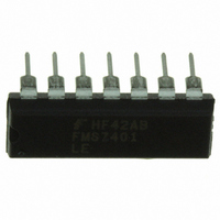
FMS7401LEN14 Fairchild Semiconductor, FMS7401LEN14 Datasheet - Page 11

FMS7401LEN14
Manufacturer Part Number
FMS7401LEN14
Description
IC CTRLR POWER DGTL EEPROM 14DIP
Manufacturer
Fairchild Semiconductor
Datasheet
1.FMS7401LVN.pdf
(81 pages)
Specifications of FMS7401LEN14
Applications
Digital Power Controller
Core Processor
8-Bit
Program Memory Type
EEPROM (1 kB)
Ram Size
64 x 8
Number Of I /o
8
Voltage - Supply
2.7 V ~ 3.6 V
Operating Temperature
-40°C ~ 85°C
Mounting Type
Through Hole
Package / Case
14-DIP (0.300", 7.62mm)
Output Current
5 mA
Input Voltage
2.7 V to 3.6 V
Switching Frequency
2 MHz
Operating Temperature Range
- 40 C to + 85 C
Mounting Style
Through Hole
Lead Free Status / RoHS Status
Lead free / RoHS Compliant
Interface
-
Controller Series
-
Lead Free Status / Rohs Status
Lead free / RoHS Compliant
Other names
FMS7401LEN14_NL
FMS7401LEN14_NL
FMS7401LEN14_NL
Available stocks
Company
Part Number
Manufacturer
Quantity
Price
Company:
Part Number:
FMS7401LEN14
Manufacturer:
Rohm
Quantity:
21 626
The FS[1:0] bits of the PSCALE register
changed by software at any time; however, if the PWM Timer 1 circuit is in run mode the FS[1:0] value will not change the
F
PWM cycle end time will dictate the divide factor of the F
the value reported will be the last value written by software (it may not necessarily reflect the divide factor for the current
PWM cycle).
The main system instruction clock (F
with the same divide factor as the FS[1:0] = 00 selection.
(if FMODE=1) or F
eight times faster than the standard. The FMODE bit may not be set if the PLL is not enabled.
FMODE while PLLEN=0 will force FMODE=0 ignoring any set instruction. Once the PLL has been enabled, software may
change F
In order to synchronously disable the PLL clocking structure, software must clear FSEL and FMODE before clearing the
PLLEN bit in order to disable the PLL successfully e.g. using separate instructions like “RBIT PLLEN, PSCALE.” There are
also special conditions for Halt/Idle power saving modes that must also be considered. Please refer to the
section of the datasheet for details.
REV. 1.0.3 1/24/05
PRODUCT SPECIFICATION
PWMCLK
C
ICLK
output frequency until after the PWM cycle ends (once the TMR1 counter overflows). The last FS[1:0] value at the
l o c k
O
I
n
s
’s source on-the-fly during normal instruction execution in order to speed-up a particular action.
I
t
N
c i l l a t o
T
e r
r
I
i
T
n
m m
2
a l
r
i
n
RCLK1
g
(
F
O
S
divided-by-2 signal. With the FMODE bit enabled, it is possible to execute instructions at a speed
C
)
F
R
C L K
1
D i
ICLK
b y 2
v
i
d e
4
) source may be provided by the internal oscillator (F
select the divide factor for the F
Figure 3. Internal Clock Scheme
R E
B
A
F
S e
Y
B Y
l
2
6
P L L
The FMODE bit of the PSCALE register
PWMCLK
F
R
E N
C L K
2
F
F
S [ 1 ]
S [ 0 ]
output for the next PWM cycle. When reading the FS[1:0],
(
F
D i g i t a l
P L L
M
u
)
(
P L L
l t i
PWMCLK
C
p
l i
l o c k
)
e r
output (see
F
(
F
F
S
P W M C L K
= 0
)
5
Table
OSC
Any attempts to write to
B
A
F
S
) or the PLL’s F
S e
4
Y
E
l
selects between the F
F
L
3). The FS bits may be
M
O
D
Power Saving Modes
E
A
B
S e
l
Y
F
T
1
C L K
(FS=0)
F
I
C L K
FMS7401L
output
(FS=0)
11


