SAA7706H/N210,518 NXP Semiconductors, SAA7706H/N210,518 Datasheet - Page 31
SAA7706H/N210,518
Manufacturer Part Number
SAA7706H/N210,518
Description
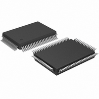
IC CAR RADIO DSP 80-QFP
Manufacturer
NXP Semiconductors
Type
Car Signal Processorr
Datasheet
1.SAA7706HN210S518.pdf
(52 pages)
Specifications of SAA7706H/N210,518
Interface
I²C, I²S, LSB, SPDIF
Voltage - I/o
3.30V
Voltage - Core
3.30V
Operating Temperature
-40°C ~ 85°C
Mounting Type
Surface Mount
Package / Case
80-QFP
Lead Free Status / RoHS Status
Lead free / RoHS Compliant
Clock Rate
-
Non-volatile Memory
-
On-chip Ram
-
Other names
935270285518
SAA7706H/N210-T
SAA7706H/N210-T
SAA7706H/N210-T
SAA7706H/N210-T
Available stocks
Company
Part Number
Manufacturer
Quantity
Price
Company:

Part Number:
SAA7706H/N210,518
Manufacturer:
NXP Semiconductors
Quantity:
10 000


Philips Semiconductors
9
For more general information on the I
the Philips I
9.1
Before any data is transmitted on the I
which should respond is addressed first. The addressing is
always done with the first byte transmitted after the start
procedure.
9.2
The SAA7706H acts as slave receiver or a slave
transmitter. Therefore the clock signal SCL is only an input
signal. The data signal SDA is a bidirectional line. The
SAA7706H slave address is shown in Table 3.
Table 3 Slave address
The sub-address bit A0 corresponds to the hardware
address pin A0 which allows the device to have 2 different
addresses. The A0 input is also used in test mode as a
serial input of the test control block.
9.3
The I
Fig.20. The write cycle is used to write the bytes to both
DSP1 and DSP2 for manipulating the data and
coefficients. Depending on which DSP is accessed the
data protocol exists out of 2, 3 or 4 bytes. More details can
be found in the I
The data length is 2, 3 or 4 bytes depending on the
accessed memory. If the Y-memory of DSP1 is addressed
the data length is 2 bytes, in the event of the X-memory of
DSP1 or X/Y-memory of DSP2 the length is 3 bytes. The
slave receiver detects the address and adjusts the number
of bytes accordingly. The data length of 4 bytes is not used
in the SAA7706H.
9.4
The I
Fig.21. The read cycle is used to read the data values from
XRAM or YRAM of both DSPs. The master starts with a
START condition S, the SAA7706H address ‘0011100’
and a logic 0 (write) for the R/W bit. This is followed by an
acknowledge of the SAA7706H.
2001 Mar 05
MSB
Car radio Digital Signal Processor (DSP)
0
I
2
2
2
C-BUS FORMAT
C-bus configuration for a write cycle is shown in
C-bus configuration for a READ cycle is shown in
Addressing
Slave address (pin A0)
Write cycles
Read cycles
0
2
C-bus specification.
2
C-bus memory map (see Table 5).
1
1
1
2
C-bus protocol, see
2
0
C-bus, the device
A0
LSB
R/W
31
Then the master writes the high memory address and low
memory address where the reading of the memory content
of the SAA7706H must start. The SAA7706H
acknowledges these addresses both. Then the master
generates a repeated START (Sr) and again the
SAA7706H address ‘0011100’ but this time followed by a
logic 1 (read) of the R/W bit.
From this moment on the SAA7706H will send the memory
content in groups of 2 (Y-memory DSP1) or 3 (X-memory
DSP1, X/Y-memory DSP2 or registers) bytes to the
I
master stops this cycle by generating a negative
acknowledge, then the SAA7706H frees the I
the master can generate a STOP condition. The data is
transferred from the DSP register to the I
execution of the MPI instruction in the DSP2 program.
Therefore at least once every DSP routine an MPI
instruction should be added. The data length of 4 bytes is
not used in the SAA7706H.
9.5
The write cycle can be used to write the bytes to the
hardware registers to control the DCS block, the PLL for
the DSP clock generation, the IAC settings, the AD volume
control settings, the analog input selection, the format of
the I
read these locations for chip status information. More
detail can be found in the I
Tables 4 and 5.
9.5.1
The hardware registers have two different address blocks.
One block exists out of hardware register locations which
control both DSPs and some major settings such as the
PLL division. These locations have a maximum of 16 bits,
which means 2 bytes need to be sent to or read from. For
the SAA7706H one register is located at the DSPs and
general control register (0FFFH).
The second block has an address space of 16 addresses
and are all X-memory mapped on DSP2. While this space
is 24 bits wide 3 bytes should be sent to or read from.
These addresses are DSP2 mapped which means an MPI
instruction is needed for accessing those locations and
there is no verifying mechanism if all addresses are really
mapped to physical registers. Therefore, all those
locations will be acknowledged even if the data is not valid.
For the SAA7706H several registers are located in this
section. A few registers are predefined for DSP2 purposes
(see Table 5).
2
C-bus each time acknowledged by the master. The
2
S-bus and some other settings. It is also possible to
SAA7706H hardware registers
SAA7706H DSP
S REGISTERS
2
C-bus memory map,
Product specification
SAA7706H
2
C-bus register at
2
C-bus and
Related parts for SAA7706H/N210,518
Image
Part Number
Description
Manufacturer
Datasheet
Request
R

Part Number:
Description:
Manufacturer:
NXP Semiconductors
Datasheet:

Part Number:
Description:
IC CAR RADIO DSP 80-QFP
Manufacturer:
NXP Semiconductors
Datasheet:
Part Number:
Description:
IC CAR RADIO DSP 80-QFP
Manufacturer:
NXP Semiconductors
Datasheet:
Part Number:
Description:
IC CAR RADIO DSP 80-QFP
Manufacturer:
NXP Semiconductors
Datasheet:

Part Number:
Description:
Digital Signal Processors & Controllers - DSP, DSC DIGITAL SIGNAL PROCESSOR
Manufacturer:
NXP Semiconductors
Part Number:
Description:
IC DSP CAR RADIO 80QFP
Manufacturer:
NXP Semiconductors
Datasheet:
Part Number:
Description:
IC DSP CAR RADIO 80QFP
Manufacturer:
NXP Semiconductors
Datasheet:
Part Number:
Description:
IC DSP CAR RADIO 80QFP
Manufacturer:
NXP Semiconductors
Datasheet:
Part Number:
Description:
IC DSP CAR RADIO 80QFP
Manufacturer:
NXP Semiconductors
Datasheet:
Part Number:
Description:
Manufacturer:
NXP Semiconductors
Datasheet:
Part Number:
Description:
Manufacturer:
NXP Semiconductors
Datasheet:
Part Number:
Description:
Manufacturer:
NXP Semiconductors
Datasheet:
Part Number:
Description:
Car Radio Digital Signal Processor Dsp
Manufacturer:
NXP Semiconductors
Datasheet:
Part Number:
Description:
Digital Signal Processors & Controllers - DSP, DSC DIRAC-1
Manufacturer:
NXP Semiconductors
Part Number:
Description:
NXP Semiconductors designed the LPC2420/2460 microcontroller around a 16-bit/32-bitARM7TDMI-S CPU core with real-time debug interfaces that include both JTAG andembedded trace
Manufacturer:
NXP Semiconductors
Datasheet: