SAA7706H/N210,518 NXP Semiconductors, SAA7706H/N210,518 Datasheet - Page 22
SAA7706H/N210,518
Manufacturer Part Number
SAA7706H/N210,518
Description
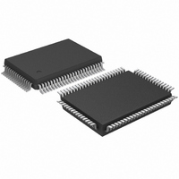
IC CAR RADIO DSP 80-QFP
Manufacturer
NXP Semiconductors
Type
Car Signal Processorr
Datasheet
1.SAA7706HN210S518.pdf
(52 pages)
Specifications of SAA7706H/N210,518
Interface
I²C, I²S, LSB, SPDIF
Voltage - I/o
3.30V
Voltage - Core
3.30V
Operating Temperature
-40°C ~ 85°C
Mounting Type
Surface Mount
Package / Case
80-QFP
Lead Free Status / RoHS Status
Lead free / RoHS Compliant
Clock Rate
-
Non-volatile Memory
-
On-chip Ram
-
Other names
935270285518
SAA7706H/N210-T
SAA7706H/N210-T
SAA7706H/N210-T
SAA7706H/N210-T
Available stocks
Company
Part Number
Manufacturer
Quantity
Price
Company:

Part Number:
SAA7706H/N210,518
Manufacturer:
NXP Semiconductors
Quantity:
10 000


Philips Semiconductors
8.7.3
With pin POM it is possible to switch off the reference
current of the DAC. The capacitor on pin POM determines
the time after which this current has a soft switch-on. So at
power-on the current audio signal outputs are always
muted. The loading of the external capacitor is done in two
stages via two different current sources. The loading starts
at a current level that is lower than the current loading after
the voltage on pin POM has past a particular level. This
results in an almost dB-linear behaviour. This must
prevent ‘plop’ effects during power on or off.
8.7.4
To avoid plops in a power amplifier, the supply voltage of
the analog part of the DAC and the rest of the chip can be
fed from a separate power supply of 3.3 V. A capacitor
connected to this power supply enables to provide power
to the analog part at the moment the digital voltage is
switching off fast. In this event the output voltage will
decrease gradually allowing the power amplifier some
extra time to switch off without audible plops.
8.7.5
With two internal resistors half the supply voltage V
obtained and used as an internal reference. This reference
voltage is used as DC voltage for the output operational
amplifiers and as reference for the DAC.
2001 Mar 05
handbook, full pagewidth
Car radio Digital Signal Processor (DSP)
F
P
P
UNCTION OF PIN
OWER
IN
VREFDA
-
OFF PLOP SUPPRESSION
FOR INTERNAL REFERENCE
POM
on-chip
off-chip
AGC
Fig.13 Block diagram oscillator circuit.
63
OSC_IN
C1
DDA2
G m
R bias
is
22
In order to obtain the lowest noise and to have the best
ripple rejection, a filter capacitor has to be added between
this pin and ground, preferably close to the analog
pin V
8.7.6
The entire analog circuitry of the DACs and the operational
amplifiers are supplied by 2 supply pins: V
V
harmonic distortion degradation and to ensure a good
power supply rejection ratio. The digital part of the DAC is
fully supplied from the chip core supply.
8.8
The chip has an on-chip crystal clock oscillator. The block
diagram of this Pierce oscillator is shown in Fig.13. The
active element needed to compensate for the loss
resistance of the crystal is the block G
placed between the external pins OSC_IN
and OSC_OUT. The gain of the oscillator is internally
controlled by the AGC block. A sine wave with a
peak-to-peak voltage close to the oscillator power supply
voltage is generated. The AGC block prevents clipping of
the sine wave and therefore the higher harmonics are as
low as possible. At the same time the voltage of the sine
wave is as high as possible which reduces the jitter going
from sine wave to the clock signal.
DDA2
64
OSC_OUT
0.5V DD(OSC)
C2
SSA2
must have sufficient decoupling to prevent total
Clock circuit and oscillator
S
.
UPPLY OF THE FILTER STREAM
65
V DD(OSC)
clock to circuit
62
V SS(OSC)
MGT469
Product specification
m
SAA7706H
DAC
. This block is
DDA2
and V
SSA2
.
Related parts for SAA7706H/N210,518
Image
Part Number
Description
Manufacturer
Datasheet
Request
R

Part Number:
Description:
Manufacturer:
NXP Semiconductors
Datasheet:

Part Number:
Description:
IC CAR RADIO DSP 80-QFP
Manufacturer:
NXP Semiconductors
Datasheet:
Part Number:
Description:
IC CAR RADIO DSP 80-QFP
Manufacturer:
NXP Semiconductors
Datasheet:
Part Number:
Description:
IC CAR RADIO DSP 80-QFP
Manufacturer:
NXP Semiconductors
Datasheet:

Part Number:
Description:
Digital Signal Processors & Controllers - DSP, DSC DIGITAL SIGNAL PROCESSOR
Manufacturer:
NXP Semiconductors
Part Number:
Description:
IC DSP CAR RADIO 80QFP
Manufacturer:
NXP Semiconductors
Datasheet:
Part Number:
Description:
IC DSP CAR RADIO 80QFP
Manufacturer:
NXP Semiconductors
Datasheet:
Part Number:
Description:
IC DSP CAR RADIO 80QFP
Manufacturer:
NXP Semiconductors
Datasheet:
Part Number:
Description:
IC DSP CAR RADIO 80QFP
Manufacturer:
NXP Semiconductors
Datasheet:
Part Number:
Description:
Manufacturer:
NXP Semiconductors
Datasheet:
Part Number:
Description:
Manufacturer:
NXP Semiconductors
Datasheet:
Part Number:
Description:
Manufacturer:
NXP Semiconductors
Datasheet:
Part Number:
Description:
Car Radio Digital Signal Processor Dsp
Manufacturer:
NXP Semiconductors
Datasheet:
Part Number:
Description:
Digital Signal Processors & Controllers - DSP, DSC DIRAC-1
Manufacturer:
NXP Semiconductors
Part Number:
Description:
NXP Semiconductors designed the LPC2420/2460 microcontroller around a 16-bit/32-bitARM7TDMI-S CPU core with real-time debug interfaces that include both JTAG andembedded trace
Manufacturer:
NXP Semiconductors
Datasheet: