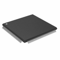
ADSP-21261SKSTZ150 Analog Devices Inc, ADSP-21261SKSTZ150 Datasheet - Page 21

ADSP-21261SKSTZ150
Manufacturer Part Number
ADSP-21261SKSTZ150
Description
IC DSP 32BIT 150MHZ 144LQFP
Manufacturer
Analog Devices Inc
Series
SHARC®r
Type
Fixed/Floating Pointr
Specifications of ADSP-21261SKSTZ150
Interface
DAI, SPI
Clock Rate
150MHz
Non-volatile Memory
ROM (384 kB)
On-chip Ram
128kB
Voltage - I/o
3.30V
Voltage - Core
1.20V
Operating Temperature
0°C ~ 70°C
Mounting Type
Surface Mount
Package / Case
144-LQFP
No. Of Bits
32 / 40
Frequency
150MHz
Supply Voltage
1.2V
Embedded Interface Type
Serial
Supply Voltage Range
1.14V To 1.26V
Operating Temperature Range
0°C To +70°C
Digital Ic
RoHS Compliant
Device Core Size
32/40Bit
Architecture
Super Harvard
Format
Floating Point
Clock Freq (max)
150MHz
Mips
150
Device Input Clock Speed
150MHz
Ram Size
128KB
Program Memory Size
384KB
Operating Supply Voltage (typ)
1.2/3.3V
Operating Supply Voltage (min)
1.14/3.13V
Operating Supply Voltage (max)
1.26/3.47V
Operating Temp Range
0C to 70C
Operating Temperature Classification
Commercial
Mounting
Surface Mount
Pin Count
144
Package Type
LQFP
Package
144LQFP
Numeric And Arithmetic Format
Floating-Point
Maximum Speed
150 MHz
Device Million Instructions Per Second
150 MIPS
Lead Free Status / RoHS Status
Lead free / RoHS Compliant
Lead Free Status / RoHS Status
Lead free / RoHS Compliant
Available stocks
Company
Part Number
Manufacturer
Quantity
Price
Company:
Part Number:
ADSP-21261SKSTZ150
Manufacturer:
Analog Devices Inc
Quantity:
10 000
Part Number:
ADSP-21261SKSTZ150
Manufacturer:
ADI/亚德诺
Quantity:
20 000
Timer WDTH_CAP Timing
The timing specification in
Timer in WDTH_CAP (pulse width count and capture) mode.
Timer signals are routed to the DAI_P20–1 pins through the
SRU. Therefore, the timing specifications provided below are
valid at the DAI_P20–1 pins.
Table 21. Timer Width Capture Timing
DAI Pin-to-Pin Direct Routing
See
example, DAI_PB01_I to DAI_PB02_O).
Table 22. DAI Pin-to-Pin Routing
Parameter
Timing Requirements
t
Parameter
Timing Requirements
t
PWI
DPIO
DAI_P20–1
Table 22
(TIMER)
and
Timer Pulse Width
Figure 13
Delay DAI Pin Input Valid to DAI Output Valid
for direct pin connections only (for
Table 21
and
Figure 12
DAI_Pm
DAI_Pn
Figure 13. DAI Pin-to-Pin Direct Routing
Figure 12. Timer Width Capture Timing
applies to
Rev. F | Page 21 of 44 | July 2009
Min
2 × t
CCLK
t
PWI
t
DPIO
ADSP-21261/ADSP-21262/ADSP-21266
Min
1.5
Max
2(2
31
– 1) × t
CCLK
Max
10
Unit
ns
Unit
ns


